Datasheet4U Logo Datasheet4U.com

NB6L11S - Input to LVDS Fanout Buffer/Translator

General Description

Pin Name I/O Description 1 Q0 LVDS Output Non

inverted D output.

Typically loaded with 100 W receiver termination resistor across differential pair.

Inverted D output.

Key Features

  • Input Clock Frequency > 2.0 GHz.
  • Input Data Rate > 2.5 Gb/s.
  • RMS Clock Jitter.
  • 0.5 ps, Typical.
  • 622 Mb/s Data Dependent Jitter.
  • 6 ps, Typical.
  • 380 ps Typical Propagation Delay.
  • 120 ps Typical Rise and Fall Times.
  • Single Power Supply; VCC = 2.5 V " 5%.
  • These are Pb.
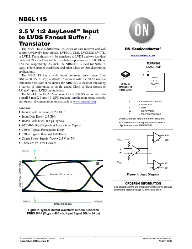
  • Free Devices Device DDJ = 10 ps www. onsemi. com 1 QFN.
  • 16 MN SUFFIX CASE 485G.

📥 Download Datasheet

Datasheet Details

Part number NB6L11S
Manufacturer onsemi
File Size 316.46 KB
Description Input to LVDS Fanout Buffer/Translator
Datasheet download datasheet NB6L11S Datasheet

Full PDF Text Transcription (Reference)

The following content is an automatically extracted verbatim text from the original manufacturer datasheet and is provided for reference purposes only.

View original datasheet text
NB6L11S VOLTAGE (130 mV/div) 2.5 V 1:2 AnyLevel] Input to LVDS Fanout Buffer / Translator The NB6L11S is a differential 1:2 clock or data receiver and will accept AnyLevel™ input signals: LVPECL, CML, LVCMOS, LVTTL, or LVDS. These signals will be translated to LVDS and two identical copies of Clock or Data will be distributed, operating up to 2.0 GHz or 2.5 Gb/s, respectively. As such, the NB6L11S is ideal for SONET, GigE, Fiber Channel, Backplane and other Clock or Data distribution applications. The NB6L11S has a wide input common mode range from GND + 50 mV to VCC − 50 mV. Combined with the 50 W internal termination resistors at the inputs, the NB6L11S is ideal for translating a variety of differential or single−ended Clock or Data signals to 350 mV typical LVDS output levels.