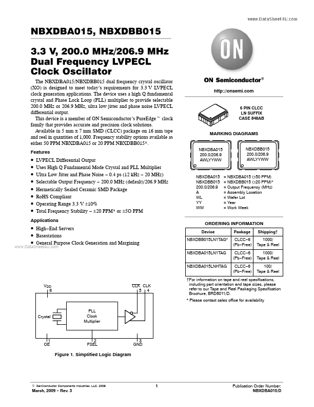
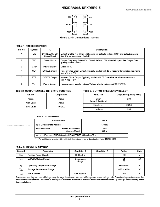
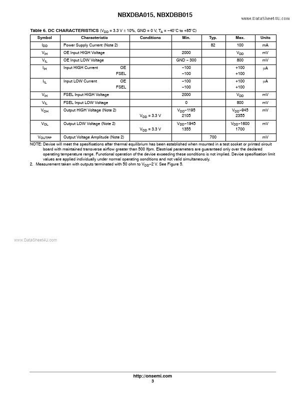
logo

NBXDBA015 Datasheet, ON Semiconductor

NBXDBA015 Datasheet, ON Semiconductor

NBXDBA015

datasheet Download (Size : 156.32KB)

NBXDBA015 Datasheet

NBXDBA015 oscillator

clock oscillator.

NBXDBA015

datasheet Download (Size : 156.32KB)

NBXDBA015 Datasheet

NBXDBA015 Features and benefits

NBXDBA015 Features and benefits

http://onsemi.com 6 PIN CLCC LN SUFFIX CASE 848AB MARKING DIAGRAMS NBXDBA015 200.0/206.9 AWLYYWW NBXDBB015 200.0/206.9 AWLYYWW
*
*
*
*
*
*
.

NBXDBA015 Application

NBXDBA015 Application

The device uses a high Q fundamental crystal and Phase Lock Loop (PLL) multiplier to provide selectable 200.0 MHz or 20.

NBXDBA015 Description

NBXDBA015 Description

Pin No. 1 2 3 4 5 6 Symbol OE FSEL GND CLK CLK VDD I/O LVTTL/LVCMOS Control Input Control Input Power Supply LVPECL Output LVPECL Output Power Supply Description Output Enable Pin. When left floating pin defaults to logic HIGH and output is active. S.

Image gallery

NBXDBA015 Page 1 NBXDBA015 Page 2 NBXDBA015 Page 3

TAGS

NBXDBA015
Clock
Oscillator
ON Semiconductor

Manufacturer


ON Semiconductor (https://www.onsemi.com/)

Related datasheet

NBXDBA012

NBXDBA014

NBXDBA017

NBXDBA018

NBXDBA019

NBXDBA009

NBXDBB015

NBXDBB017

NBXDBB018

NBXDDA016

NBXDDB016

NBXDPA012

NBXDPA017

Since 2006. D4U Semicon.   |   Contact Us   |   Privacy Policy   |   Purchase of parts