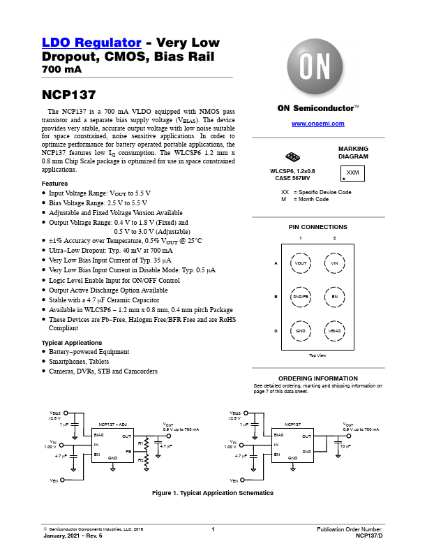
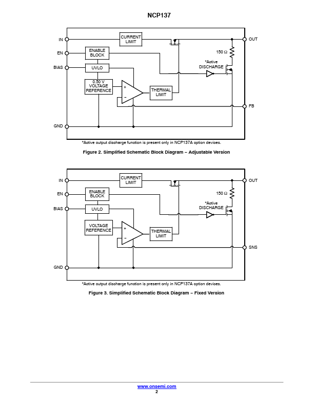
NCP137 Description
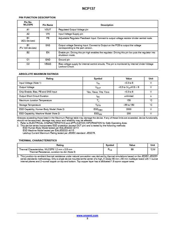
WLCSP6 Pin Name Description A1 VOUT Regulated Output Voltage pin A2 VIN Input Voltage Supply pin B1 (ADJ devices) FB Adjustable Regulator Feedback Input. Connect to output voltage resistor divider central node. B1 (Fix Volt devices) SNS Output voltage Sensing Input.
NCP137 Applications
- Input Voltage Range: VOUT to 5.5 V
- Bias Voltage Range: 2.5 V to 5.5 V
- Adjustable and Fixed Voltage Version Available
- Output Voltage Range: 0.4 V to 1.8 V (Fixed) and