NCP1392D
NCP1392D is High-Voltage Half-Bridge Driver manufactured by onsemi.
Features
- Wide Operating Frequency Range
- from 25 k Hz to 480 k Hz
- Minimum frequency adjust accuracy $3%
- Fixed Dead Time
- 0.6 ms or 0.3 ms
- Adjustable Brown- out Protection for a Simple PFC Association
- 100 ms or 12.6 ms PFC Delay Timer
- Non- latched Enable Input
- Internal 16 V VCC Clamp
- Low Startup Current of 50 m A
- 1 A / 0.5 A Peak Current Sink / Source Drive Capability
- Operation up to 600 V Bulk Voltage
- Internal Temperature Shutdown
- SOIC- 8 Package
- These are Pb- Free Devices
Typical Applications
- Flat Panel Display Power Converters
- Low Cost Resonant SMPS
- High Power AC/DC Adapters for Notebooks
- Offline Battery Chargers
- Lamp Ballasts
.onsemi.
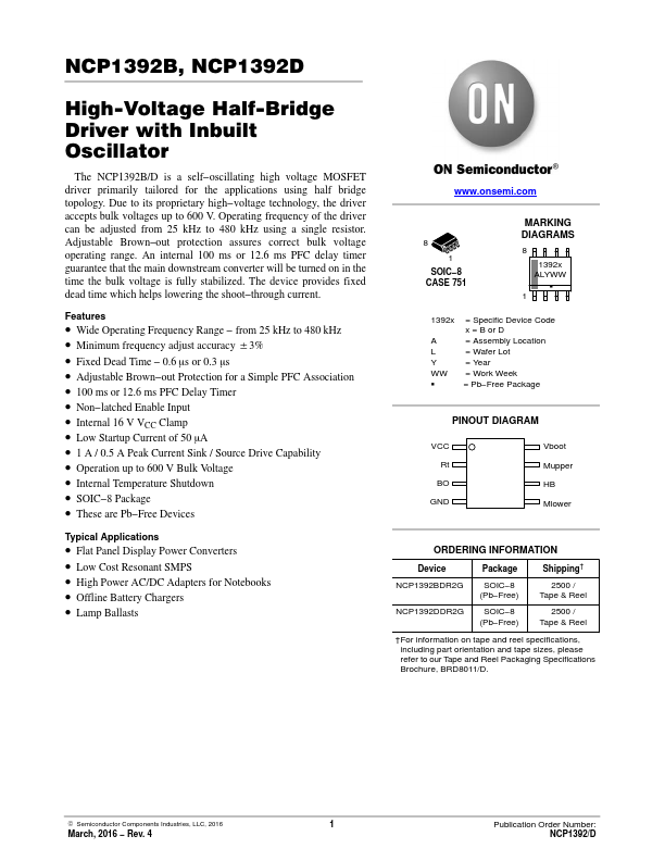
1 SOIC- 8 CASE 751
MARKING DIAGRAMS
1392x ALYWW
G 1
1392x
A L Y WW G
= Specific Device Code x = B or D = Assembly Location = Wafer Lot = Year = Work Week = Pb- Free Package
PINOUT DIAGRAM
VCC Rt BO
Vboot Mupper HB Mlower
ORDERING INFORMATION
Device
Package
Shipping†...