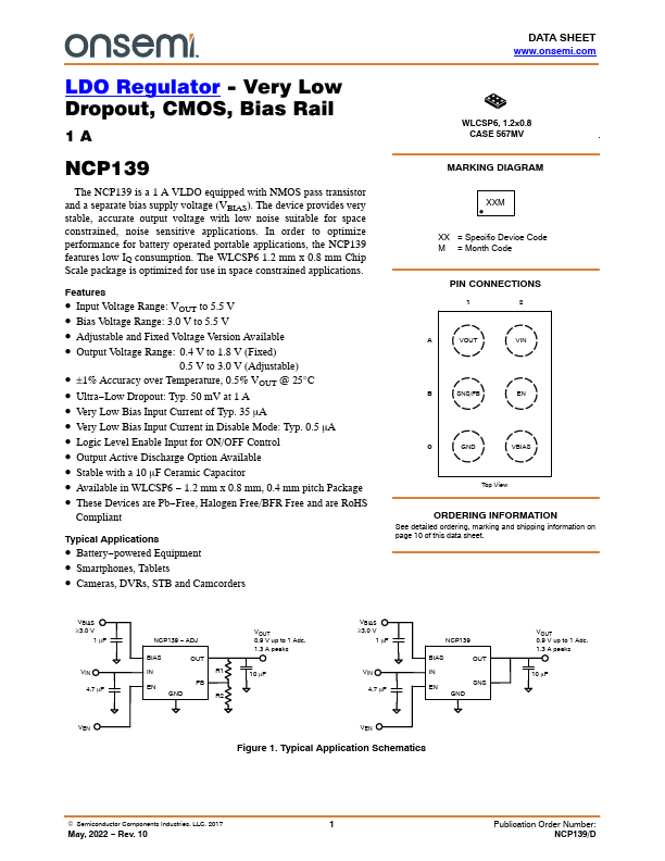
Datasheet4U Logo Datasheet4U.com

NCP139 - LDO Regulator

General Description

Pin No.

Description Regulated Output Voltage pin Input Voltage Supply pin Adjustable Regulator Feedback Input.

Connect to output voltage resistor divider central node.

Key Features

  • low IQ consumption. The WLCSP6 1.2 mm x 0.8 mm Chip Scale package is optimized for use in space constrained.

📥 Download Datasheet

Datasheet Details

Part number NCP139
Manufacturer onsemi
File Size 536.42 KB
Description LDO Regulator
Datasheet download datasheet NCP139 Datasheet

Full PDF Text Transcription (Reference)

The following content is an automatically extracted verbatim text from the original manufacturer datasheet and is provided for reference purposes only.

View original datasheet text
LDO Regulator - Very Low Dropout, CMOS, Bias Rail 1A NCP139 
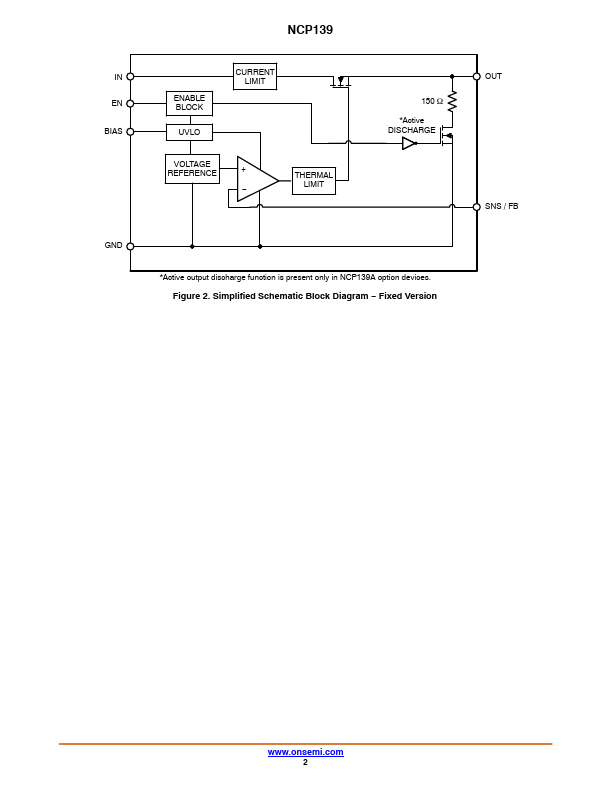
The NCP139 is a 1 A VLDO equipped with NMOS pass transistor and a separate bias supply voltage (VBIAS). The device provides very stable, accurate output voltage with low noise suitable for space constrained, noise sensitive applications. In order to optimize performance for battery operated portable applications, the NCP139 features low IQ consumption. The WLCSP6 1.2 mm x 0.8 mm Chip Scale package is optimized for use in space constrained applications. Features • Input Voltage Range: VOUT to 5.5 V • Bias Voltage Range: 3.0 V to 5.5 V • Adjustable and Fixed Voltage Version Available • Output Voltage Range: 0.4 V to 1.8 V (Fixed) Output Voltage Range 0.5 V to 3.0 V (Adjustable) • ±1% Accuracy over Temperature, 0.