NCP1393B
Overview
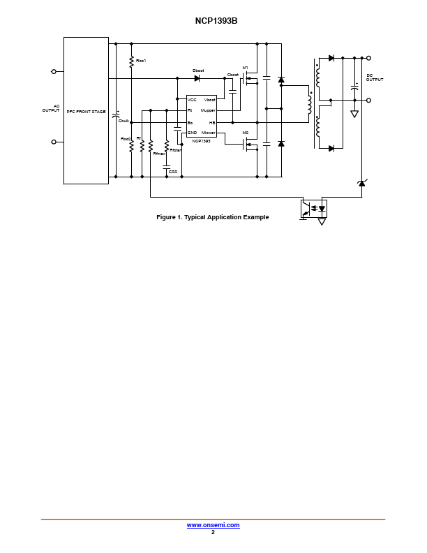
NCP1393B Rbo1 Dboot M1 Cboot AC OUTPUT PFC FRONT STAGE + VCC Vboot Rt Mupper Cbulk Bo HB Rbo2 Rf GND Mlower M2 NCP1393 Rfstart Rfmax CSS Figure 1. Typical Application Example DC OUTP...
| Part | NCP1393B |
|---|---|
| Description | High-Voltage Half-Bridge Driver |
| Manufacturer | onsemi |
| Size | 282.97 KB |
NCP1393B Rbo1 Dboot M1 Cboot AC OUTPUT PFC FRONT STAGE + VCC Vboot Rt Mupper Cbulk Bo HB Rbo2 Rf GND Mlower M2 NCP1393 Rfstart Rfmax CSS Figure 1. Typical Application Example DC OUTP...
| Part Number | Manufacturer | Description |
|---|---|---|
| OB3375 | On-Bright | High performance buck LED driver |
| NSi6602 | NOVOSENSE | High Reliability Isolated Dual-Channel Gate Driver |
| BP2861X | BPS | step-down LED constant current driver |