Datasheet Summary
..
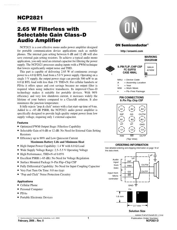
NCP2821 2.65 W Filterless with Selectable Gain Class- D Audio Amplifier
NCP2821 is a cost effective mono audio power amplifier designed for portable munication device applications such as mobile phones. The internal gain setting between 6 dB and 12 dB will also save external gain setting resistors. To achieve a typical audio mono application, you only need an external capacitor for filtering the power supply. The NCP2821 processes analog inputs with a PWM technique that lowers significantly output noise and THD. This part is capable of delivering 2.65 W of continuous average power to a 4.0 W BTL load from a 5.0 V power supply. Operating on a single 3 V supply, the...