NCP3488
NCP3488 is MOSFET Driver manufactured by onsemi.
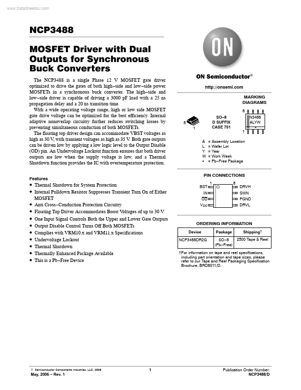
Features http://onsemi. MARKING DIAGRAMS
8 8 1 A L Y W G SO- 8 D SUFFIX CASE 751 N3488 ALYW G
= Assembly Location = Wafer Lot = Year = Work Week = Pb- Free Package
PIN CONNECTIONS
BST IN OD VCC 1 8 DRVH SWN PGND DRVL
- Thermal Shutdown for System Protection
- Internal Pulldown Resistor Suppresses Transient Turn On of Either
- -
- -
- -
- -
- MOSFET Anti Cross- Conduction Protection Circuitry Floating Top Driver Acmodates Boost Voltages of up to 30 V One Input Signal Controls Both the Upper and Lower Gate Outputs Output Disable Control Turns Off Both MOSFETs plies with VRM10.x and VRM11.x Specifications Undervoltage Lockout Thermal Shutdown Thermally Enhanced Package Available This is a Pb- Free Device
ORDERING INFORMATION
Device NCP3488DR2G Package SO- 8 (Pb- Free) Shipping † 2500 Tape & Reel
†For information on tape and reel specifications, including part orientation and tape sizes, please refer to our Tape and Reel Packaging Specification Brochure, BRD8011/D.
© Semiconductor ponents Industries, LLC, 2006
May, 2006
- Rev. 1
Publication Order Number: NCP3488/D
OD 3 V CC TSD UVLO IN 2 8 DRVH 1 BST
FALLING EDGE DELAY FALLING EDGE DELAY START STOP NON- OVERLAP TIMERS
MONITOR 7 MONITOR SWN
MIN DRVL OFF TIMER
4 5 6
V CC DRVL PGND
Figure 1. Block Diagram
PIN DESCRIPTION
Pin No. 1 Symbol BST Description
Upper MOSFET Floating Bootstrap Supply. A capacitor connected between BST and SW pins holds this bootstrap voltage for the high- side MOSFET as it is switched. The remended capacitor value is between 100 n F and 1.0 m F. An external diode is required with the NCP3488. Logic- Level Input. This pin has primary control of the drive outputs. Output Disable. When low, normal operation is disabled forcing DRVH and DRVL low. Input Supply. A 1.0 m F ceramic capacitor should be connected from this pin to PGND. Output drive for the lower MOSFET. Power Ground. Should be closely connected to the source of the...