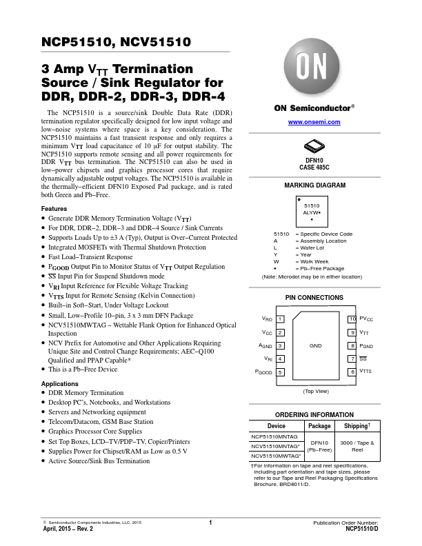
NCP51510 Description
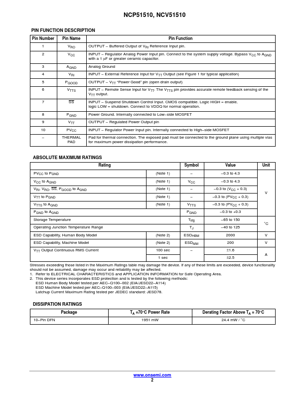
Pin Number Pin Name Pin Function 1 VRO OUTPUT − Buffered Output of VRI Reference Input pin. 2 VCC INPUT − Regulator Analog Power Input pin. Connect to the system supply voltage.
NCP51510 Key Features
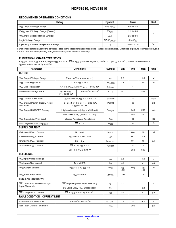
- Generate DDR Memory Termination Voltage (VTT)
- For DDR, DDR-2, DDR-3 and DDR-4 Source / Sink Currents
- Supports Loads Up to ±3 A (Typ), Output is Over-Current Protected
- Integrated MOSFETs with Thermal Shutdown Protection
- Fast Load-Transient Response
- PGOOD Output Pin to Monitor Status of VTT Output Regulation
- SS Input Pin for Suspend Shutdown mode
- VRI Input Reference for Flexible Voltage Tracking
- VTTS Input for Remote Sensing (Kelvin Connection)
- Built-in Soft-Start, Under Voltage Lockout