NCP5369N
Integrated Driver and
MOSFET
The NCP5369N integrates a MOSFET driver, high−side MOSFET
and low−side MOSFET into a 6 mm x 6 mm 40−pin QFN package.
The driver and MOSFETs have been optimized for high−current
DC−DC buck power conversion applications. The NCP5369N
integrated solution greatly reduces package parasitics and board space
compared to a discrete component solution.
Features
• Capable of Switching Frequencies Up to 1 MHz
• Capable of Output Currents Up to 35 A
• Internal Bootstrap Diode
• Zero Current Detection
• Undervoltage Lockout
• Internal Thermal Warning / Thermal Shutdown
• These are Pb−Free Devices
5 V 12−20 V
5V
GL Control
Output
Disable
PWM
Thermal
Warning
THWN
VIN
VCIN
BOOT
SMOD
DISB#
PWM
CGND
PHASE
VSWH
PGND
Vout
http://onsemi.com
1 40
QFN40
MN SUFFIX
CASE 485AZ
MARKING
DIAGRAM
1
NCP5369N
AWLYYWWG
A = Assembly Location
WL = Wafer Lot
YY = Year
WW = Work Week
G = Pb−Free Package
ORDERING INFORMATION
Device
Package
Shipping†
NCP5369NMNTXG QFN40 2500/Tape & Reel
(Pb−Free)
†For information on tape and reel specifications,
including part orientation and tape sizes, please
refer to our Tape and Reel Packaging Specification
Brochure, BRD8011/D.
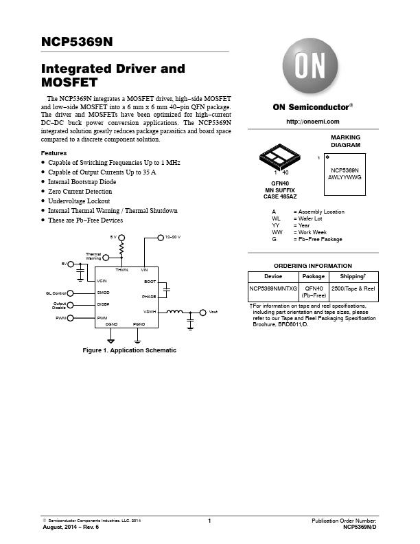
Figure 1. Application Schematic
© Semiconductor Components Industries, LLC, 2014
August, 2014 − Rev. 6
1
Publication Order Number:
NCP5369N/D