NCP5369
NCP5369 is Integrated Driver MOSFET manufactured by onsemi.
Integrated Driver and MOSFET
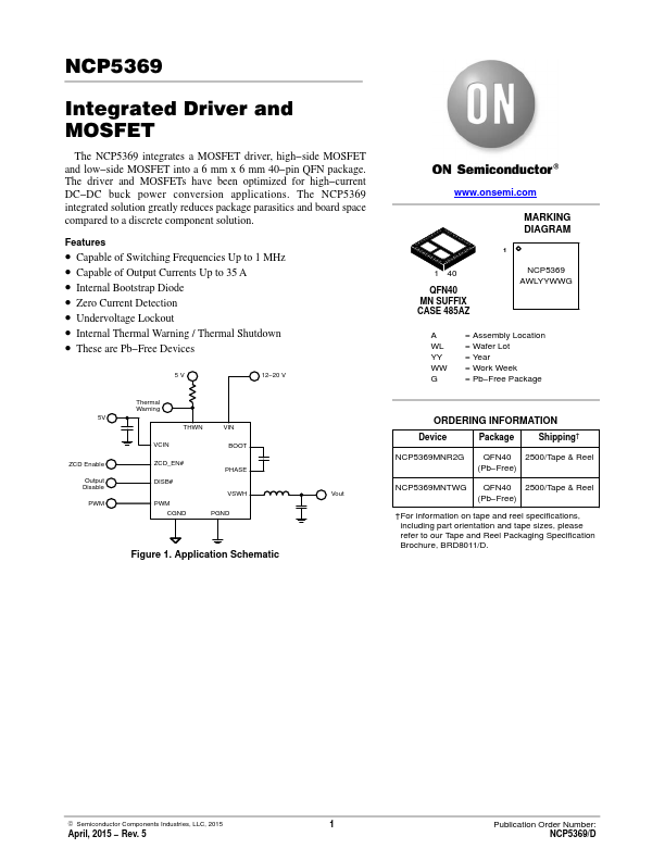
The NCP5369 integrates a MOSFET driver, high- side MOSFET and low- side MOSFET into a 6 mm x 6 mm 40- pin QFN package. The driver and MOSFETs have been optimized for high- current DC- DC buck power conversion applications. The NCP5369 integrated solution greatly reduces package parasitics and board space pared to a discrete ponent solution.
Features
- Capable of Switching Frequencies Up to 1 MHz
- Capable of Output Currents Up to 35 A
- Internal Bootstrap Diode
- Zero Current Detection
- Undervoltage Lockout
- Internal Thermal Warning / Thermal Shutdown
- These are Pb- Free Devices
5 V 12- 20 V
5V
ZCD Enable Output Disable PWM
Thermal...