NCP5369N
Description
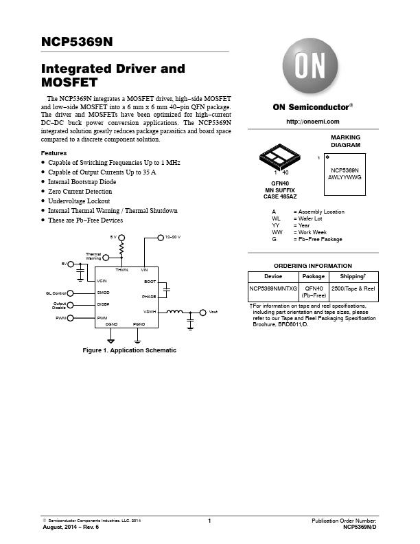
1 SMOD GL Control 2 VCIN Control Input Voltage 3, 8 NC No Connect 4 BOOT Bootstrap Voltage 5, 37, FLAG 41 CGND Control Signal Ground 6 GH High Side FET Gate Access 7 PHASE Provides a return path for the high side driver of the internal IC.
Key Features
- Capable of Switching Frequencies Up to 1 MHz
- Capable of Output Currents Up to 35 A
- Internal Bootstrap Diode
- Zero Current Detection
- Undervoltage Lockout