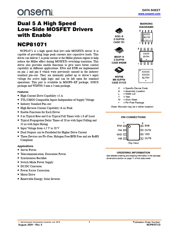
NCP81071 Overview
Key Features
- High Current Drive Capability ±5 A
- TTL/CMOS Compatible Inputs Independent of Supply Voltage
- Industry Standard Pin-out
- High Reverse Current Capability (6 A) Peak
- Enable Functions for Each Driver
- 8 ns Typical Rise and 8 ns Typical Fall Times with 1.8 nF Load
- Typical Propagation Delay Times of 20 ns with Input Falling and 20 ns with Input Rising
- Input Voltage from 4.5 V to 20 V
- Dual Outputs can be Paralleled for Higher Drive Current
- These Devices are Pb-Free, Halogen Free/BFR Free and are RoHS Compliant