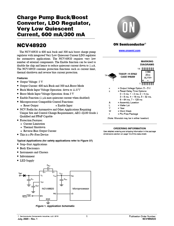
Datasheet4U Logo Datasheet4U.com

NCV48920 - LDO Regulator

Description

Pin No.

Charge Pump Output Voltage (Input Voltage of LDO).

Not Connected.

Flying Capacitor Negative Connection.

Charge Pump Input Voltage.

Features

  • Output Voltage: 5 V.
  • Output Current: 600 mA Buck and 300 mA Boost Mode.
  • Buck Mode Input Voltage Operation: down to 11.8 V.
  • Boost Mode Input Voltage Operation: from 3 V.
  • Enable Function (1 mA max quiescent current when disabled).
  • Microprocessor Compatible Control Functions:.
  • Reset Output.
  • Enable Input.
  • NCV Prefix for Automotive and Other.

📥 Download Datasheet

Datasheet preview – NCV48920

Datasheet Details

Part number NCV48920
Manufacturer ON Semiconductor
File Size 321.41 KB
Description LDO Regulator
Datasheet download datasheet NCV48920 Datasheet
Additional preview pages of the NCV48920 datasheet.
Other Datasheets by ON Semiconductor

Full PDF Text Transcription

Click to expand full text
Charge Pump Buck/Boost Converter, LDO Regulator, Very Low Quiescent Current, 600 mA/300 mA NCV48920 The NCV48920 is 600 mA buck and 300 mA boost charge pump regulator with integrated Very Low Quiescent Current LDO regulator for automotive applications. The NCV48920 requires very low number of external components. The Enable function can be used to disable the chip and hence to reduce quiescent current down to 1 mA. The NCV48920 contains protection functions such as current limit, thermal shutdown and reverse bias current protection. Features • Output Voltage: 5 V • Output Current: 600 mA Buck and 300 mA Boost Mode • Buck Mode Input Voltage Operation: down to 11.
Published: |