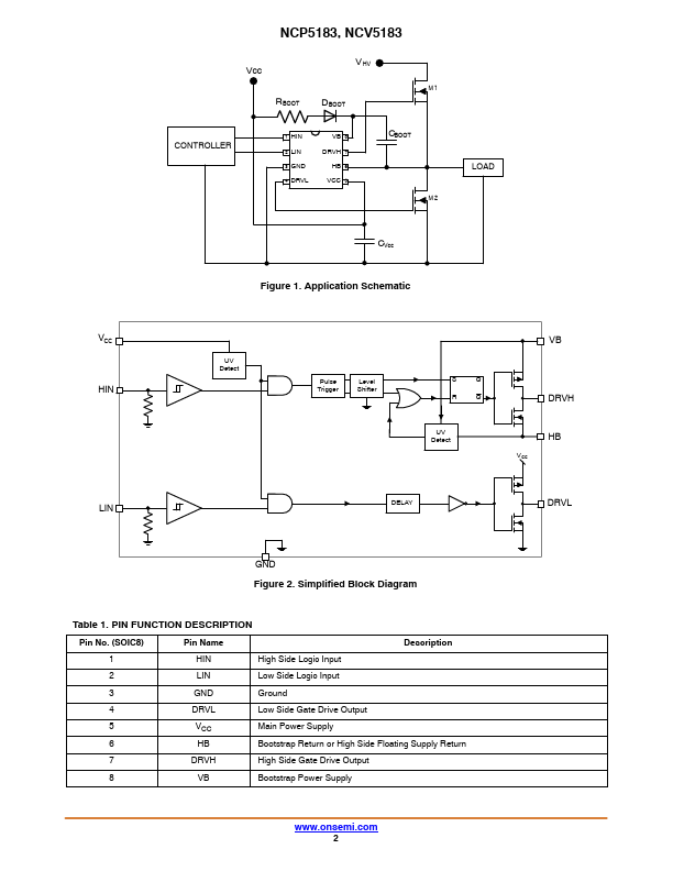
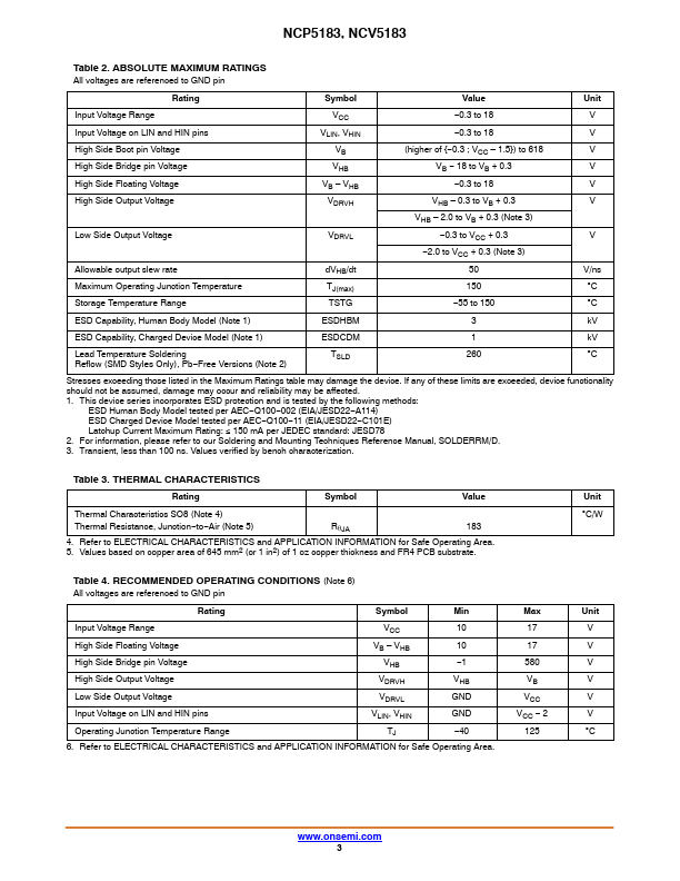
Datasheet4U Logo Datasheet4U.com

NCV5183 - High Voltage High Current High and Low Side Driver

General Description

Pin No.

Key Features

  • Automotive Qualified to AEC Q100.
  • Voltage Range: up to 600 V.
  • dV/dt Immunity 50 V/ns.
  • Gate Drive Supply Range from 9 V to 18 V.
  • Output Source / Sink Current Capability 4.3 A / 4.3 A.
  • 3.3 V and 5 V Input Logic Compatible.
  • Extended Allowable Negative Bridge Pin Voltage Swing to.
  • 10 V  Matched Propagation Delays between Both Channels  Propagation Delay 120 ns typically  Under VCC LockOut (UVLO) for Both Channels.
  • Pin to Pin Compatible with Indust.

📥 Download Datasheet

Datasheet Details

Part number NCV5183
Manufacturer onsemi
File Size 552.80 KB
Description High Voltage High Current High and Low Side Driver
Datasheet download datasheet NCV5183 Datasheet

Full PDF Text Transcription (Reference)

The following content is an automatically extracted verbatim text from the original manufacturer datasheet and is provided for reference purposes only.

View original datasheet text
High Voltage High Current High and Low Side Driver NCP5183, NCV5183 The NCP5183 is a High Voltage High Current Power MOSFET Driver providing two outputs for direct drive of two N−channel power MOSFETs arranged in a half−bridge (or any other high−side + low−side) configuration. It uses the bootstrap technique to insure a proper drive of the High−side power switch. The driver works with two independent inputs to accommodate any topology (including half−bridge, asymmetrical half−bridge, active clamp and full−bridge…). Features  Automotive Qualified to AEC Q100  Voltage Range: up to 600 V  dV/dt Immunity 50 V/ns  Gate Drive Supply Range from 9 V to 18 V  Output Source / Sink Current Capability 4.3 A / 4.3 A  3.