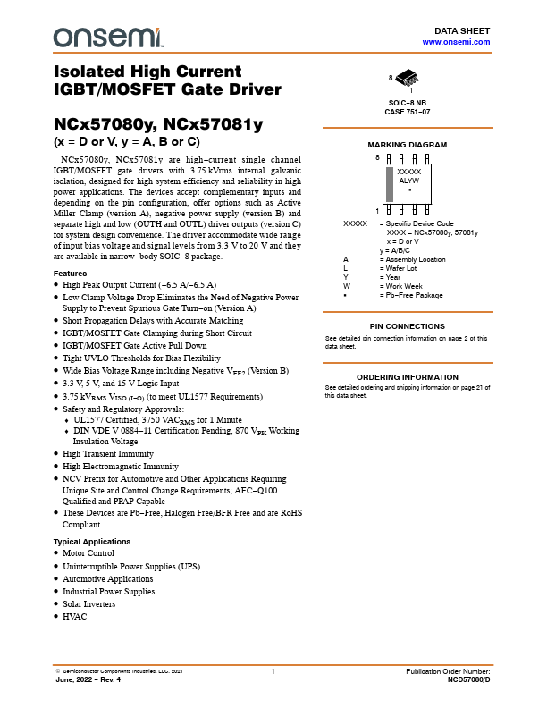
NCV57081B
Overview
- High Peak Output Current (+6.5 A/-6.5 A)
- Low Clamp Voltage Drop Eliminates the Need of Negative Power Supply to Prevent Spurious Gate Turn-on (Version A)
- Short Propagation Delays with Accurate Matching
- IGBT/MOSFET Gate Clamping during Short Circuit
- IGBT/MOSFET Gate Active Pull Down
- Tight UVLO Thresholds for Bias Flexibility
- Wide Bias Voltage Range including Negative VEE2 (Version B)
- 3.3 V, 5 V, and 15 V Logic Input
- 3.75 kVRMS VISO (I-O) (to meet UL1577 Requirements)
- Safety and Regulatory Approvals: