Datasheet Summary
NLSF1174 Hex D Flip- Flop with mon Clock and Reset
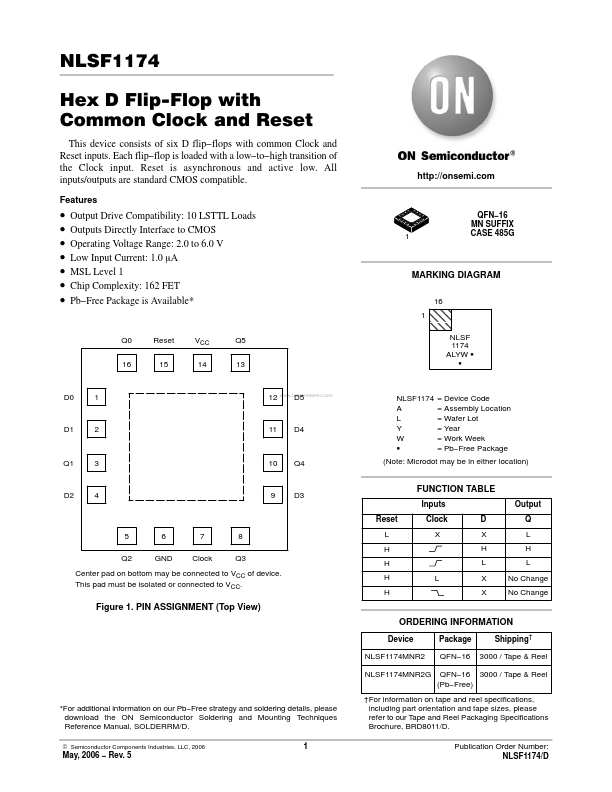
This device consists of six D flip- flops with mon Clock and Reset inputs. Each flip- flop is loaded with a low- to- high transition of the Clock input. Reset is asynchronous and active low. All inputs/outputs are standard CMOS patible.
Features http://onsemi.
- -
- -
- -
- Output Drive patibility: 10 LSTTL Loads Outputs Directly Interface to CMOS Operating Voltage Range: 2.0 to 6.0 V Low Input Current: 1.0 mA MSL Level 1 Chip plexity: 162 FET Pb- Free Package is Available-
QFN- 16 MN SUFFIX CASE 485G
MARKING DIAGRAM
Q0 16
Reset 15
VCC 14
Q5 13
ÇÇÇ ÇÇÇ
16 1 12 .. D5 NLSF1174 A L Y W G
NLSF 1174 ALYW...