NLSF308
NLSF308 is Quad 2-Input AND Gate manufactured by onsemi.
NLSF308 Quad 2- Input AND Gate
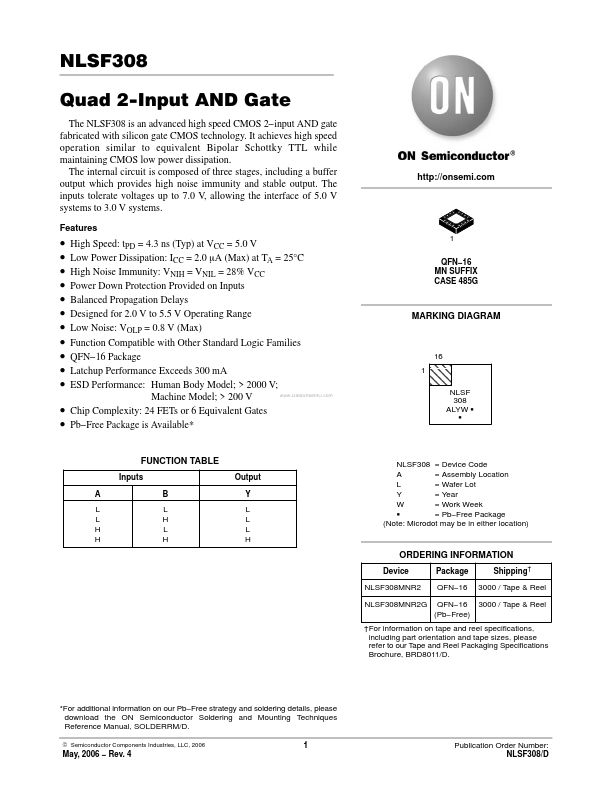
The NLSF308 is an advanced high speed CMOS 2- input AND gate fabricated with silicon gate CMOS technology. It achieves high speed operation similar to equivalent Bipolar Schottky TTL while maintaining CMOS low power dissipation. The internal circuit is posed of three stages, including a buffer output which provides high noise immunity and stable output. The inputs tolerate voltages up to 7.0 V, allowing the interface of 5.0 V systems to 3.0 V systems.
Features http://onsemi.
- -
- -
- -
- -
- -
- -
- High Speed: t PD = 4.3 ns (Typ) at VCC = 5.0 V Low Power Dissipation: ICC = 2.0 m A (Max) at TA = 25°C High Noise Immunity: VNIH = VNIL = 28% VCC Power Down Protection Provided on Inputs Balanced Propagation Delays Designed for 2.0 V to 5.5 V Operating Range Low Noise: VOLP = 0.8 V (Max) Function patible with Other Standard Logic Families QFN- 16 Package Latchup Performance Exceeds 300 m A ESD Performance: Human Body Model; > 2000 V; .. Machine Model; > 200 V Chip plexity: 24 FETs or 6 Equivalent Gates Pb- Free Package is Available-
1 QFN- 16 MN SUFFIX CASE 485G
MARKING DIAGRAM
ÇÇÇ ÇÇÇ ÇÇÇ
16 1
NLSF 308 ALYW G G
FUNCTION TABLE
Inputs A L L H H B L H L H Output Y L L L H
NLSF308 = Device Code A = Assembly Location L = Wafer Lot Y = Year W = Work Week G = Pb- Free Package (Note: Microdot may be in either location)
ORDERING INFORMATION
Device NLSF308MNR2 NLSF308MNR2G Package QFN- 16 QFN- 16 (Pb- Free) Shipping† 3000 / Tape & Reel 3000 / Tape & Reel
†For information on tape and reel specifications, including part orientation and tape sizes, please refer to our Tape and Reel Packaging Specifications Brochure, BRD8011/D.
- For additional information on our Pb- Free strategy and soldering details, please download the ON Semiconductor Soldering and Mounting Techniques Reference Manual, SOLDERRM/D.
© Semiconductor ponents Industries, LLC, 2006
May, 2006
- Rev. 4
Publication Order Number: NLSF308/D
VCC...


