NLSX3012
NLSX3012 is Translator manufactured by onsemi.
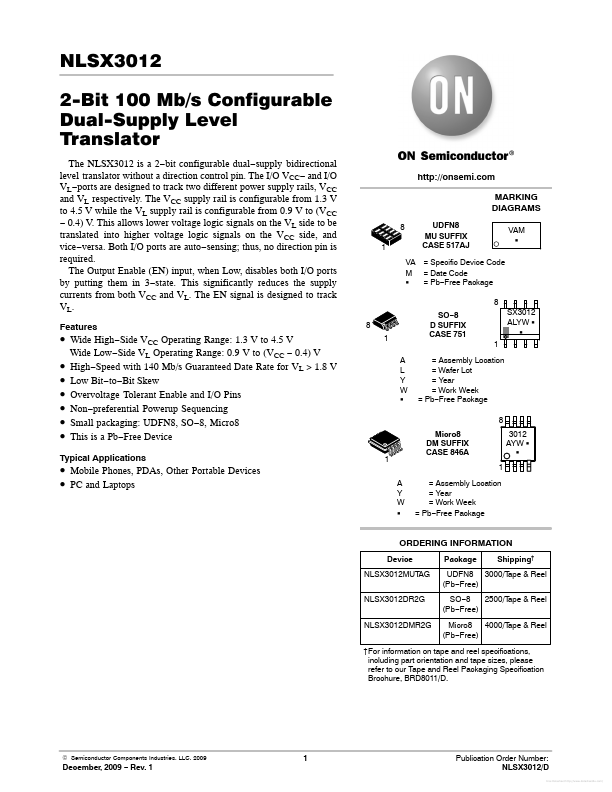
Y W G http://onsemi. MARKING DIAGRAMS
8 1 UDFN8 MU SUFFIX CASE 517AJ VA = Specific Device Code M = Date Code G = Pb- Free Package 8 SO- 8 D SUFFIX CASE 751 SX3012 ALYW G G 1 VAM G
- Wide High- Side VCC Operating Range: 1.3 V to 4.5 V
- -
- -
- -
Wide Low- Side VL Operating Range: 0.9 V to (VCC
- 0.4) V High- Speed with 140 Mb/s Guaranteed Date Rate for VL > 1.8 V Low Bit- to- Bit Skew Overvoltage Tolerant Enable and I/O Pins Non- preferential Powerup Sequencing Small packaging: UDFN8, SO- 8, Micro8 This is a Pb- Free Device
= Assembly Location = Wafer Lot = Year = Work Week = Pb- Free Package 8 Micro8 DM SUFFIX CASE 846A 1 3012 AYW G G
Typical Applications
- Mobile Phones, PDAs, Other Portable Devices
- PC and Laptops
= Assembly Location = Year = Work Week = Pb- Free Package
ORDERING INFORMATION
Device NLSX3012MUTAG NLSX3012DR2G NLSX3012DMR2G Package Shipping† UDFN8 3000/T ape & Reel (Pb- Free) SO- 8 2500/T ape & Reel (Pb- Free) Micro8 4000/T ape & Reel (Pb- Free)
†For information on tape and reel specifications, including part orientation and tape sizes, please refer to our Tape and Reel Packaging Specification Brochure, BRD8011/D.
© Semiconductor ponents Industries, LLC, 2009
December, 2009
- Rev. 1
Publication Order Number: NLSX3012/D
Free Datasheet http://../
LOGIC DIAGRAM
EN VL VCC GND
I/O VL1
I/O VCC1
I/O VL2
I/O VCC2
PIN ASSIGNMENTS
VL I/O VL1 I/O VL2 GND 1 2 3 4 UDFN8 (Top View) 8 7 6 5 VCC I/O VCC1 I/O VCC2 EN VL 1 I/O VL1 2 I/O VL2 3 GND 4 SOIC- 8 (Top View) 8 7 6 5 VCC I/O VCC1 I/O VCC2 EN VL I/O VL1 I/O VL2 GND 1 2 3 4 Micro8 (Top View) 8 7 6 5 VCC I/O VCC1 I/O VCC2 EN
PIN...