NLSX4014
NLSX4014 is Translator manufactured by onsemi.
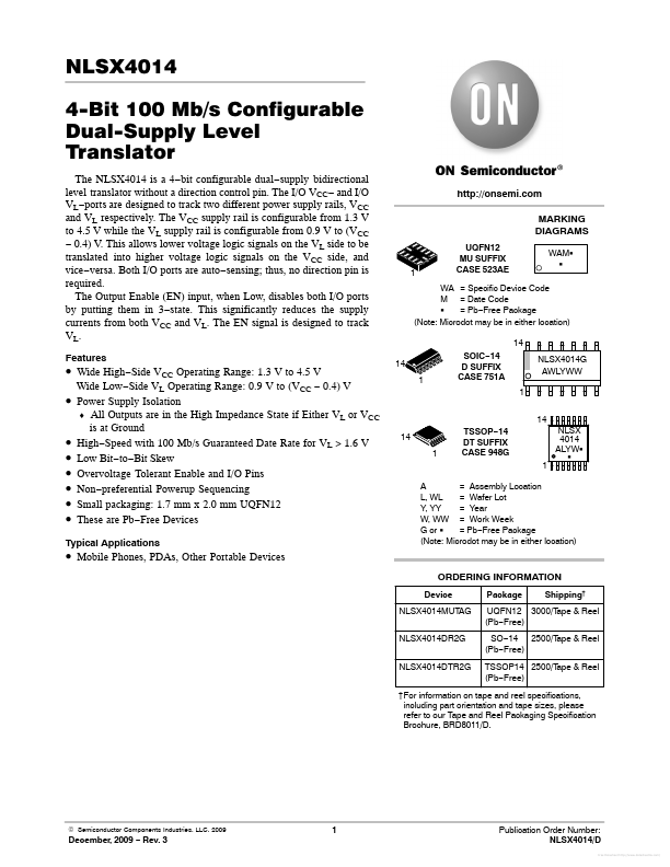
onsemi. MARKING DIAGRAMS
UQFN12 MU SUFFIX CASE 523AE WAMG G
WA = Specific Device Code M = Date Code G = Pb- Free Package (Note: Microdot may be in either location) 14 14 1 SOIC- 14 D SUFFIX CASE 751A 1 14 14 1 TSSOP- 14 DT SUFFIX CASE 948G 1 NLSX 4014 ALYWG G NLSX4014G AWLYWW
- Wide High- Side VCC Operating Range: 1.3 V to 4.5 V
- -
- -
- -
- Wide Low- Side VL Operating Range: 0.9 V to (VCC
- 0.4) V Power Supply Isolation
- All Outputs are in the High Impedance State if Either VL or VCC is at Ground High- Speed with 100 Mb/s Guaranteed Date Rate for VL > 1.6 V Low Bit- to- Bit Skew Overvoltage Tolerant Enable and I/O Pins Non- preferential Powerup Sequencing Small packaging: 1.7 mm x 2.0 mm UQFN12 These are Pb- Free Devices
Typical Applications
A = Assembly Location L, WL = Wafer Lot Y, YY = Year W, WW = Work Week G or G = Pb- Free Package (Note: Microdot may be in either location)
- Mobile Phones, PDAs, Other Portable Devices
ORDERING INFORMATION
Device NLSX4014MUTAG NLSX4014DR2G NLSX4014DTR2G Package Shipping† UQFN12 3000/T ape & Reel (Pb- Free) SO- 14 2500/T ape & Reel (Pb- Free) TSSOP14 2500/T ape & Reel (Pb- Free)
†For information on tape and reel specifications, including part orientation and tape sizes, please refer to our Tape and Reel Packaging Specification Brochure, BRD8011/D.
© Semiconductor ponents Industries, LLC, 2009
December, 2009
- Rev. 3
Publication Order Number: NLSX4014/D
Free Datasheet http://../
VL EN VL I/O VL1 I/O VL2 I/O VL3 I/O VL4
1 2 3 4 5 6 12 11 10 9 8 7
1 2 3 4 5 6 7
14 13 12 11 10 9 8
EN VCC I/O VCC1 I/O VCC2 I/O VCC3 NC I/O VCC4
VCC I/O VCC1 I/O VCC2 I/O VCC3 I/O VCC4
I/O VL1 I/O VL2 I/O VL3 I/O VL4 NC GND
GND (Top View)
Figure 1. Pin...