NLSX4373
NLSX4373 is Translator manufactured by onsemi.
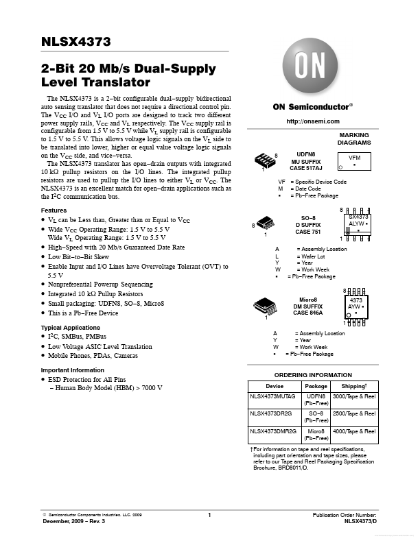
ttp://onsemi. MARKING DIAGRAMS
8 1 UDFN8 MU SUFFIX CASE 517AJ VF = Specific Device Code M = Date Code G = Pb- Free Package 8 8 1 A L Y W G SO- 8 D SUFFIX CASE 751 SX4373 ALYW G G 1 VFM G
- VL can be Less than, Greater than or Equal to VCC
- Wide VCC Operating Range: 1.5 V to 5.5 V
- -
- -
- -
- Wide VL Operating Range: 1.5 V to 5.5 V High- Speed with 20 Mb/s Guaranteed Date Rate Low Bit- to- Bit Skew Enable Input and I/O Lines have Overvoltage Tolerant (OVT) to 5.5 V Nonpreferential Powerup Sequencing Integrated 10 k W Pullup Resistors Small packaging: UDFN8, SO- 8, Micro8 This is a Pb- Free Device
= Assembly Location = Wafer Lot = Year = Work Week = Pb- Free Package 8 Micro8 DM SUFFIX CASE 846A 1 4373 AYW G G
1 A Y W G
Typical Applications
- I2C, SMBus, PMBus
- Low Voltage ASIC Level Translation
- Mobile Phones, PDAs, Cameras
Important Information
= Assembly Location = Year = Work Week = Pb- Free Package
- ESD Protection for All Pins
ORDERING INFORMATION
Device NLSX4373MUTAG NLSX4373DR2G NLSX4373DMR2G Package Shipping† UDFN8 3000/T ape & Reel (Pb- Free) SO- 8 2500/T ape & Reel (Pb- Free) Micro8 4000/T ape & Reel (Pb- Free)
- Human Body Model (HBM) > 7000 V
†For information on tape and reel specifications, including part orientation and tape sizes, please refer to our Tape and Reel Packaging Specification Brochure, BRD8011/D.
© Semiconductor ponents Industries, LLC, 2009
December, 2009
- Rev. 3
Publication Order Number: NLSX4373/D
Free Datasheet http://../
LOGIC DIAGRAM
EN VL VCC GND
I/O VL1
I/O...