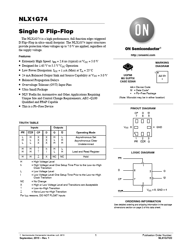
NLX1G74 Key Features
- Extremely High Speed: tPD = 2.6 ns (typical) at VCC = 5.0 V
- Designed for 1.65 V to 5.5 V VCC Operation
- Low Power Dissipation: ICC = 1 mA (Max) at TA = 25°C
- 24 mA Balanced Output Sink and Source Capability at VCC = 3.0 V
- Balanced Propagation Delays
- Overvoltage Tolerant (OVT) Input Pins
- Ultra Small Package
- NLV Prefix for Automotive and Other