NTD4860N
NTD4860N is Power MOSFET manufactured by onsemi.
Features
- ăTrench Technology
- ăLow RDS(on) to Minimize Conduction Losses
- ăLow Capacitance to Minimize Driver Losses
- ăOptimized Gate Charge to Minimize Switching Losses
- ăThese are Pb-Free Devices
Applications http://onsemi.
V(BR)DSS 25 V
RDS(ON) MAX 7.5 m W @ 10 V 11.1 m W @ 4.5 V D
ID MAX 65 A
- ăVCORE Applications
- ăDC-DC Converters
- ăHigh/Low Side Switching
MAXIMUM RATINGS (TJ = 25°C unless otherwise stated)
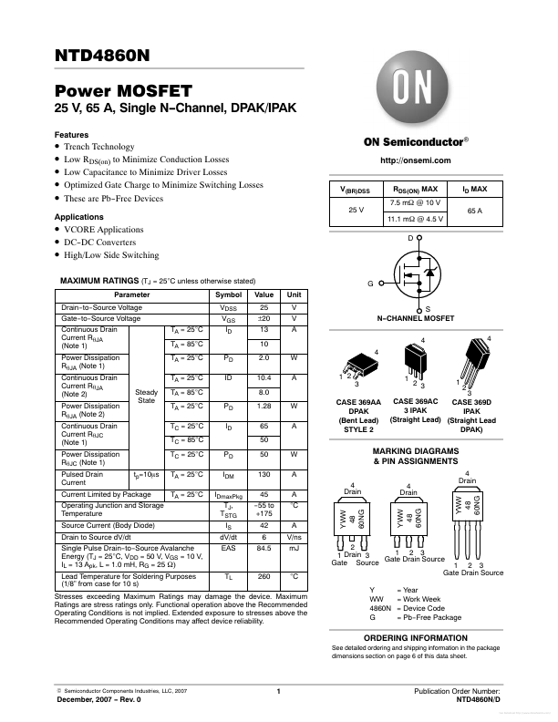
Parameter Drain-to-Source Voltage Gate-to-Source Voltage Continuous Drain Current Rq JA (Note 1) Power Dissipation Rq JA (Note 1) Continuous Drain Current Rq JA (Note 2) Power Dissipation Rq JA (Note 2) Continuous Drain Current Rq JC (Note 1) Power Dissipation Rq JC (Note 1) Pulsed Drain Current tp=10ms Steady State TA = 25°C TA = 85°C TA = 25°C TA = 25°C TA = 85°C TA = 25°C TC = 25°C TC = 85°C TC = 25°C TA = 25°C TA = 25°C PD IDM IDmax Pkg TJ, TSTG IS d V/dt EAS PD ID PD ID Symbol VDSS VGS ID Value 25 ±20 13 10 2.0 10.4 8.0 1.28 65 50 50 130 45 -55 to +175 42 6 84.5 W A A °C A V/ns m J 4 Drain YWW 48 60NG W A CASE 369AA DPAK (Bent Lead) STYLE 2 W A 1 2 3 4 Unit V V A G
S N-CHANNEL MOSFET 4 4
2 3 CASE 369AC CASE 369D 3 IPAK IPAK (Straight Lead) (Straight Lead DPAK)
2 3
MARKING DIAGRAMS & PIN ASSIGNMENTS
4 Drain YWW 48 60NG 4 Drain YWW 48 60NG
Free Datasheet http://../
Current Limited by Package Operating Junction and Storage Temperature Source Current (Body Diode) Drain to Source d V/dt
Single Pulse Drain-to-Source Avalanche Energy (TJ = 25°C, VDD = 50 V, VGS = 10 V, IL = 13 Apk, L = 1.0 m H, RG = 25 W) Lead Temperature for Soldering Purposes (1/8” from case for 10 s)
°C
2 1 2 3 1 Drain 3 Gate Source Gate Drain Source 1 2 3 Gate Drain Source Y WW 4860N G = Year = Work Week = Device Code = Pb-Free Package
Stresses exceeding Maximum Ratings may damage the device. Maximum Ratings are stress ratings only. Functional operation above the Remended Operating Conditions is not implied. Extended exposure to stresses above the Remended Operating...