NVD5117PL Overview
Key Specifications
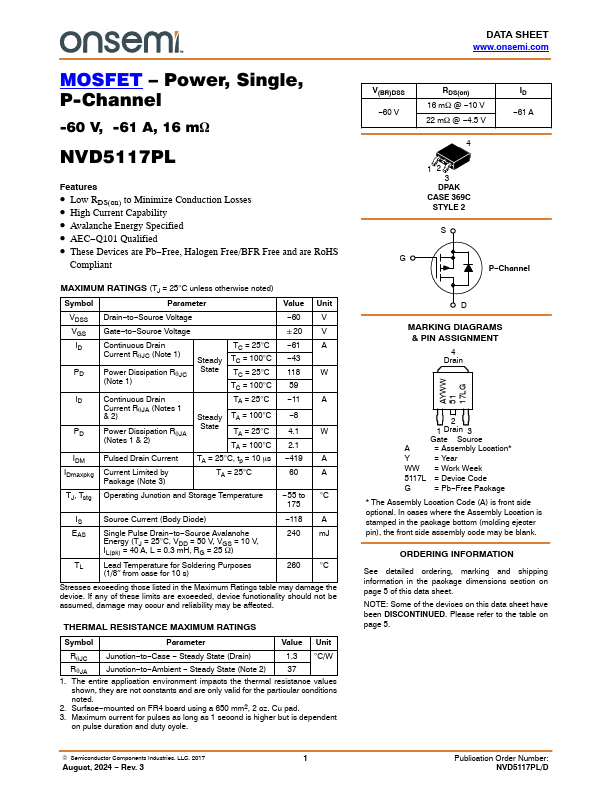
Package: DPAK
Height: 2.51 mm
Max Operating Temp: 175 °C
Min Operating Temp: -55 °C
Key Features
- Low RDS(on) to Minimize Conduction Losses
- High Current Capability
- Avalanche Energy Specified
- AEC-Q101 Qualified
- These Devices are Pb-Free, Halogen Free/BFR Free and are RoHS Compliant