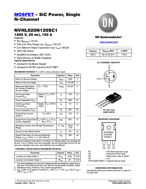
NVHL020N120SC1 Overview
MOSFET - SiC Power, Single N-Channel NVHL020N120SC1 1200 V, 20 mW, 103.
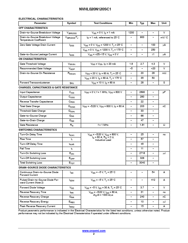
NVHL020N120SC1 Key Features
- Typ. RDS(on) = 20 mW
- Ultra Low Gate Charge (typ. QG(tot) = 203 nC)
- Low Effective Output Capacitance (typ. Coss = 260 pF)
- 100% UIL Tested
- Qualified According to AEC-Q101
- These Devices are RoHS pliant