P2N2907A Description
P2N2907A Amplifier Transistor PNP Silicon.
P2N2907A Key Features
- These are Pb--Free Devices
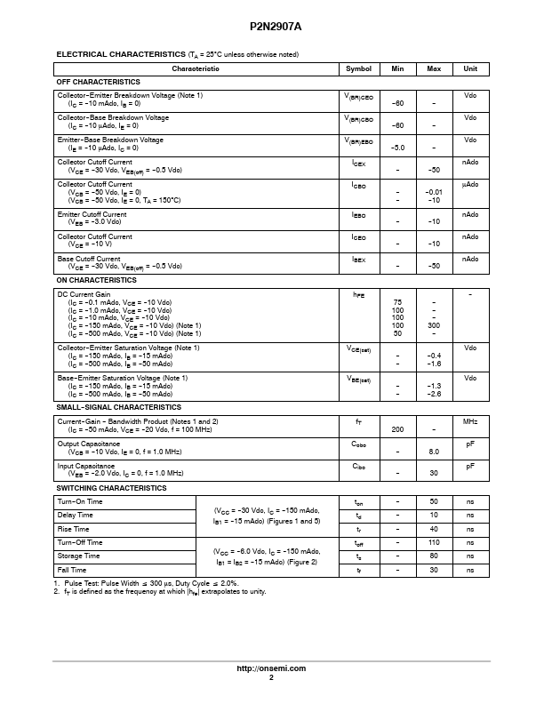
- 55 to +150
P2N2907A is Amplifier Transistor manufactured by onsemi .
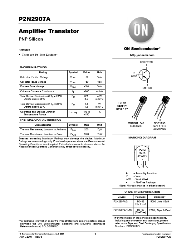
P2N2907A Amplifier Transistor PNP Silicon.