Datasheet4U Logo Datasheet4U.com

PCS3P622Z09B Datasheet – Peak EMI Reduction IC

Manufacturer: onsemi

Download the PCS3P622Z09B datasheet PDF. This datasheet also includes the PCS3P622Z05B variant, as both parts are published together in a single manufacturer document.

📥 Download Datasheet

Note: The manufacturer provides a single datasheet file (PCS3P622Z05B-ONSemiconductor.pdf) that lists specifications for multiple related part numbers.

General Description

PCS3P622Z05/09 is a versatile, 3.3 V Zero−delay buffer designed to distribute low frequency Timing−Safe clocks with Peak EMI reduction.

PCS3P622Z05 is an eight−pin version, accepts one reference input and drives out five low−skew Timing−Safe clocks.

PCS3P622Z09 accepts one reference input and drives out nine low−skew Timing−Safe clocks.

Overview

PCS3P622Z05B, PCS3P622Z05C, PCS3P622Z09B, PCS3P622Z09C Product Preview Low Frequency TIMING SAFEt Peak EMI Reduction.

Key Features

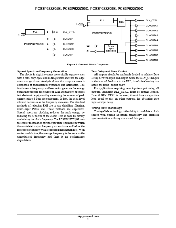
  • Low Frequency Clock Distribution with Timing.
  • Safe Peak EMI Reduction.
  • Input Frequency Range: 4 MHz.
  • 20 MHz.
  • Multiple Low Skew Timing.
  • Safe Outputs: PCS3P622Z05: 5 Outputs PCS3P622Z09: 9 Outputs.
  • External Input.
  • Output Delay Control Option.
  • Supply Voltage: 3.3 V ± 0.3 V.
  • Commercial and Industrial Temperature Range.
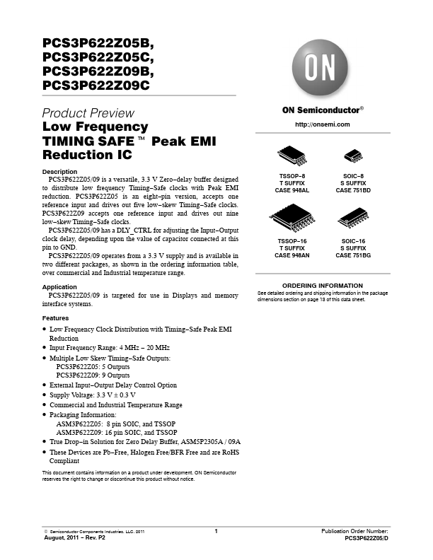
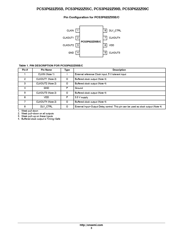
  • Packaging Information: ASM3P622Z05: 8 pin SOIC, and TSSOP ASM3P622Z09: 16 pin SOIC, and T.