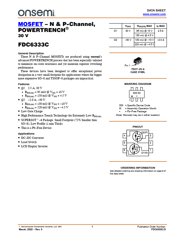
Datasheet4U Logo Datasheet4U.com

FDC6333C - N- & P-Channel Power MOSFET

Description

These N & P Channel MOSFETs are produced using onsemi’s advanced POWERTRENCH process that has been especially tailored to minimize on

state resistance and yet maintain superior switching performance.

Features

  • Q1 2.5 A, 30 V.
  • RDS(on) = 95 mW @ VGS = 10 V.
  • RDS(on) = 150 mW @ VGS = 4.5 V.
  • Q2.
  • 2.0 A,.
  • 30 V.
  • RDS(on) = 130 mW @ VGS =.
  • 10 V.
  • RDS(on) = 220 mW @ VGS =.
  • 4.5 V.
  • Low Gate Charge.
  • High Performance Trench Technology for Extremely Low RDS(on).
  • SUPERSOTt.
  • 6 Package: Small Footprint (72% Smaller than SO.
  • 8); Low Profile (1 mm Thick).
  • This is a Pb.
  • Free Device.

📥 Download Datasheet

Datasheet Details

Part number FDC6333C
Manufacturer onsemi
File Size 361.06 KB
Description N- & P-Channel Power MOSFET
Datasheet download datasheet FDC6333C Datasheet

Full PDF Text Transcription (Reference)

The following content is an automatically extracted verbatim text from the original manufacturer datasheet and is provided for reference purposes only.

View original datasheet text
MOSFET – N & P-Channel, POWERTRENCH) 30 V FDC6333C General Description These N & P−Channel MOSFETs are produced using onsemi’s advanced POWERTRENCH process that has been especially tailored to minimize on−state resistance and yet maintain superior switching performance. These devices have been designed to offer exceptional power dissipation in a very small footprint for applications where the bigger more expensive SO−8 and TSSOP−8 packages are impractical. Features • Q1 2.5 A, 30 V ♦ RDS(on) = 95 mW @ VGS = 10 V ♦ RDS(on) = 150 mW @ VGS = 4.5 V • Q2 −2.0 A, −30 V ♦ RDS(on) = 130 mW @ VGS = −10 V ♦ RDS(on) = 220 mW @ VGS = −4.
Published: |