FDC6333C Overview
Key Specifications
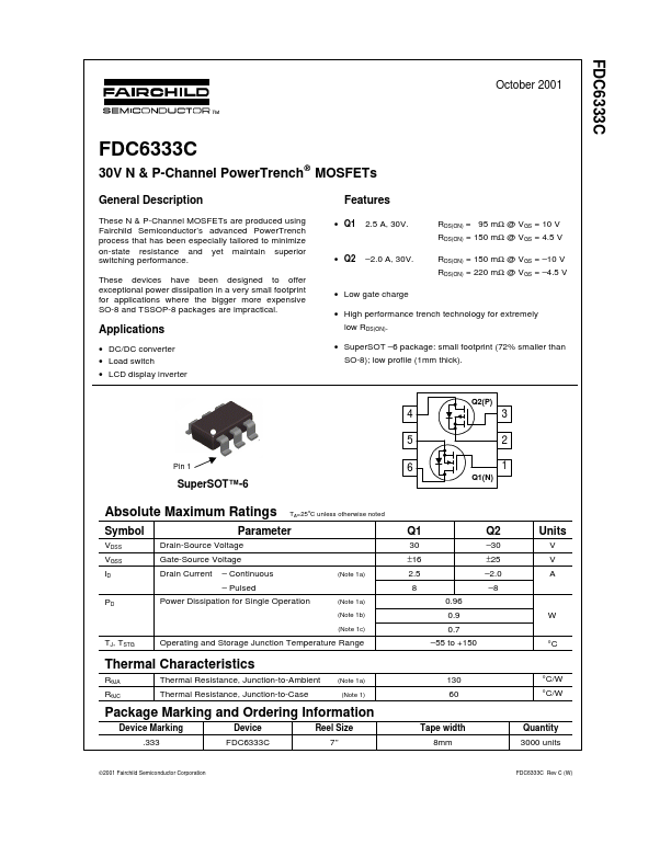
Package: SOT-23-6
Mount Type: Surface Mount
Pins: 6
Height: 1 mm
Description
These N & P-Channel MOSFETs are produced using Fairchild Semiconductor’s advanced PowerTrench process that has been especially tailored to minimize on-state resistance and yet maintain superior switching performance. These devices have been designed to offer exceptional power dissipation in a very small footprint for applications where the bigger more expensive SO-8 and TSSOP-8 packages are impractical.
Key Features
- Q1 2.5 A, 30V. RDS(ON) = 95 mΩ @ VGS = 10 V RDS(ON) = 150 mΩ @ VGS = 4.5 V
- Q2 –2.0 A, 30V. RDS(ON) = 150 mΩ @ VGS = –10 V RDS(ON) = 220 mΩ @ VGS = –4.5 V
- Low gate charge
- High performance trench technology for extremely low RDS(ON)
- SuperSOT –6 package: small footprint (72% smaller than SO-8); low profile (1mm thick)