Datasheet Summary
FQ D 60N07
60V N-Channel MOSFET
General Description
The FQD60N07 used advanced trench technology to provide excellent RDS(ON) and low gate charge. Those devices are suitable for use as a load switch or in PWM applications.
Product Summary
VDS ID (at VGS=10V) RDS(ON) (at VGS=10V) RDS(ON) (at VGS = 5V)
60V 60A
< 18mΩ
< 25mΩ
100% UIS Tested 100% Rg Tested
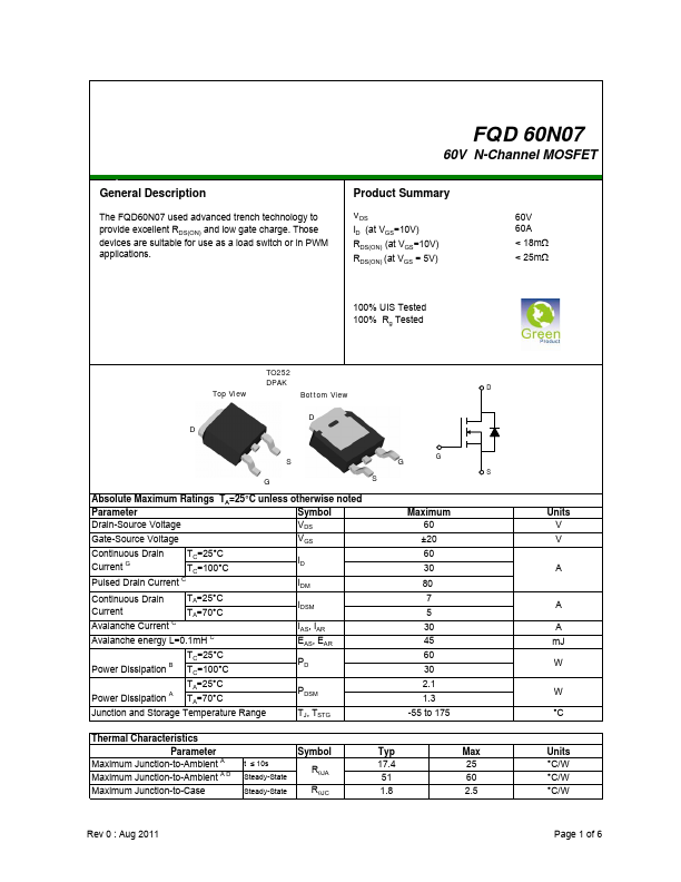
Top View D
TO252 DPAK
Bottom...