Datasheet Summary
60V N-Channel MOSFET
General Description
Product Summary
The FQD12N06bine advanced trench MOSFET technology with a low resistance package to provide extremely low RDS(ON). Those devices are suitable for use in PWM, load switching and general purpose applications.
VDS ID (at VGS=10V) RDS(ON) (at VGS=10V) RDS(ON) (at VGS = 4.5V)
100% UIS Tested 100% Rg Tested
60V 12A
< 65mΩ
< 85mΩ
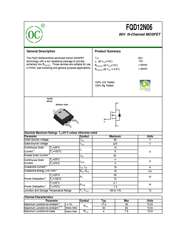
TO252 DPAK
Bottom...