PYA28C16B
PYA28C16B is EEPROM manufactured by PYRAMID.
FEATURES
Access Times of 150, 200, 250 and 350ns Single 5V±10% Power Supply
Byte Write Cycle Time
- 10 ms Maximum
Low Power CMOS:
- 60 m A Active Current
- 150 µA Standby Current
Fast Write Cycle Time
- DATA Polling CMOS & TTL patible Inputs and Outputs
2K X 8 EEPROM
Endurance:
- 10,000 Write Cycles
- 100,000 Write Cycles (optional)
Data Retention: 10 Years
Available in the following package:
- 24-Pin 600 mil Ceramic DIP
- 32-Pin Ceramic LCC (450x550 mils)
DESCRIPTION
The PYA28C16B is a 5 Volt 2Kx8 EEPROM. The PYA28C16B is a 16K memory organized as 2,048 words by 8 bits. Data Retention is 10 Years. The device is available in a 24-Pin 600 mil wide Ceramic DIP and 32-Pin LCC.
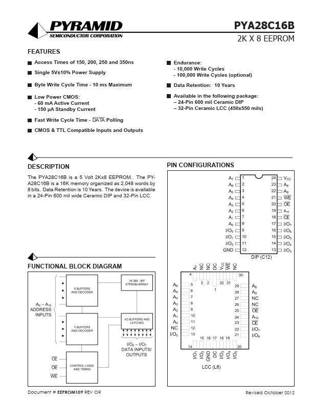
PIN CONFIGURATIONS
FUNCTIONAL BLOCK DIAGRAM
DIP (C12)
Document # EEPROM109 REV OR
LCC (L6)
Revised October 2012
- 2K x 8 EEPROM
OPERATION
READ Read operations are initiated by both OE and CE LOW. The read operation is terminated by either CE or OE returning HIGH. This two line control architecture eliminates bus contention in a system environment. The data bus will be in a high impedance state when either OE or CE is HIGH.
BYTE WRITE Write operations are initiated when both CE and WE are LOW and OE is HIGH. The PYA28C16B supports both a CE and WE controlled write cycle. That is, the address is latched by the falling edge of either CE or WE, whichever occurs last. Similarly, the data is latched internally by the rising edge of either CE or WE, whichever occurs first. A byte write operation, once initiated, will automatically continue to pletion.
CHIP CLEAR The contents of the entire memory of the PYA28C16B may be set to the high state by the CHIP CLEAR operation. By setting CE low and OE to 12 volts, the chip is cleared when a 10 msec low pulse is applied to WE.
DEVICE IDENTIFICATION An extra 32 bytes of EEPROM memory are available to the user for device identification. By raising A9 to 12 ± 0.5V and using address locations 7E0H to 7FFH the...