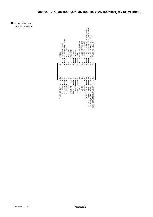
MN101CD0A Description
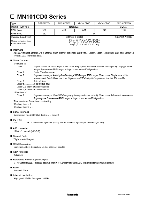
External 6 (key interrupt dedicated). A/D conversion finish Timer Counter 8-bit timer × 5 Timer 0 ..................Square-wave/8-bit PWM output. Simple pulse width measurement.
MN101CD0A is Microcontroller manufactured by Panasonic.
| Part Number | Description |
|---|---|
| MN101CD0C | Microcontroller |
| MN101CD0D | Microcontroller |
| MN101CD0G | Microcontroller |
| MN101C01 | Microcontroller |
| MN101C115 | (MN101CP115 / MN101CP117) LSI User Manual |
External 6 (key interrupt dedicated). A/D conversion finish Timer Counter 8-bit timer × 5 Timer 0 ..................Square-wave/8-bit PWM output. Simple pulse width measurement.