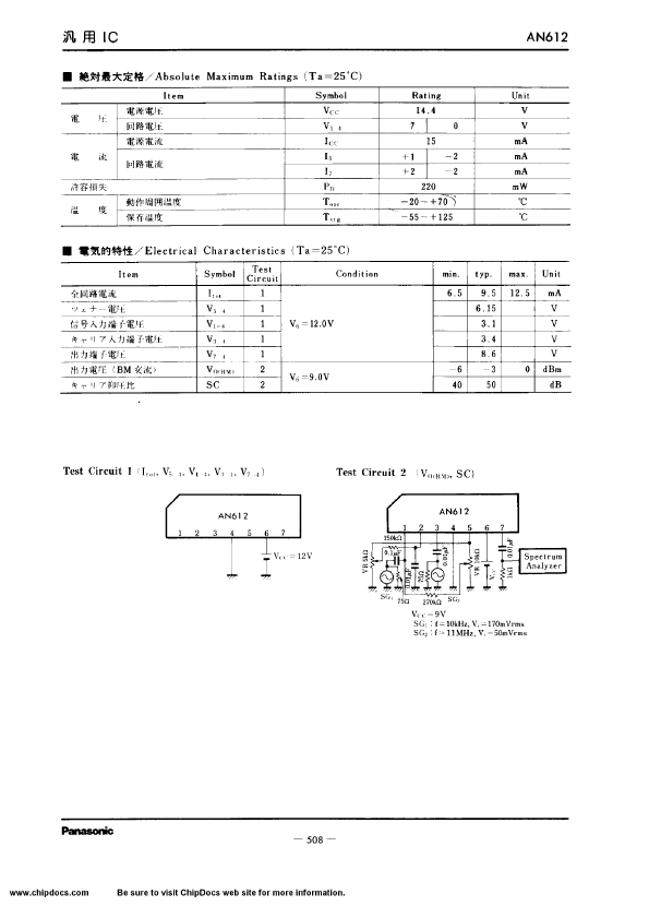
Datasheet Specifications
- Part number
- AN612
- Manufacturer
- Panasonic Semiconductor
- File Size
- 48.80 KB
- Datasheet
- AN612_PanasonicSemiconductor.pdf
- Description
- Balance Modulator Circuit
Description
WIRELESS, RF, AND CABLE Jun 01, 2001 TD-SCDMA Radio Chipset Block Diagram for Handset Application China option for 3G cellular phone is the TD-SCDMA.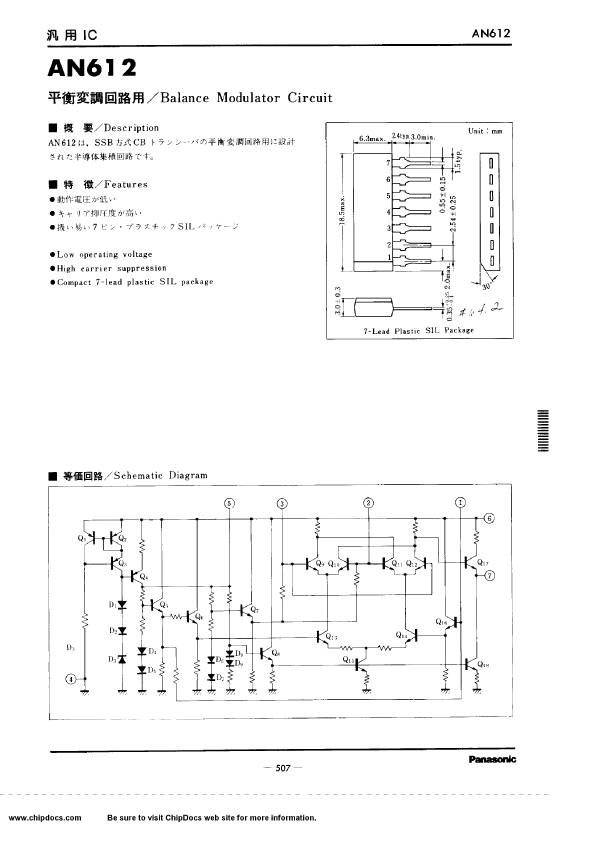
Features
* q q q q Output power of +8dBm with excellent ACPR A 100dB power-control range Dual integer-N synthesizers for IF and RF An image-reject upconverting mixer, which saves one SAW filter q q q Power-supply current dropping as the RF output power is reduced Low-noise power during the power-down modeAN612 Distributors
📁 Related Datasheet
📌 All Tags