D1251A
Key Features
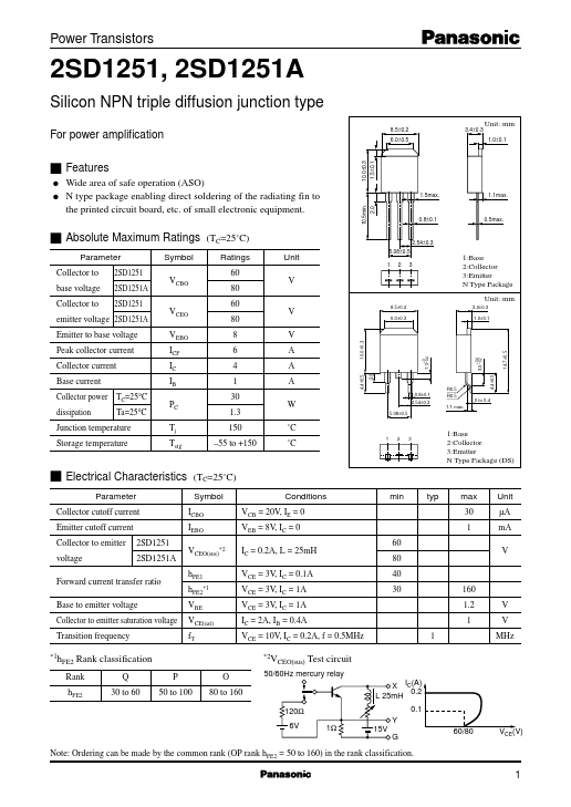
- q Wide area of safe operation (ASO) q N type package enabling direct soldering of the radiating fin to
- 1 VBE VCE(sat) fT
- 1hFE2 Rank classification
- 2VCEO(sus) Test circuit
| Part Number | Manufacturer | Description |
|---|---|---|
| D1251S45T | eupec | Fast Diode |
| D125FF08 | Voltage Multipliers | RECTIFIER DIODE |
| D125FF06 | Voltage Multipliers | RECTIFIER DIODE |
| D125F06 | Voltage Multipliers | RECTIFIER DIODE |
| D125F08 | Voltage Multipliers | RECTIFIER DIODE |
| D125F10 | Voltage Multipliers | RECTIFIER DIODE |
| D1257 | Panasonic | 2SD1257 |