PI90LVT211
Overview
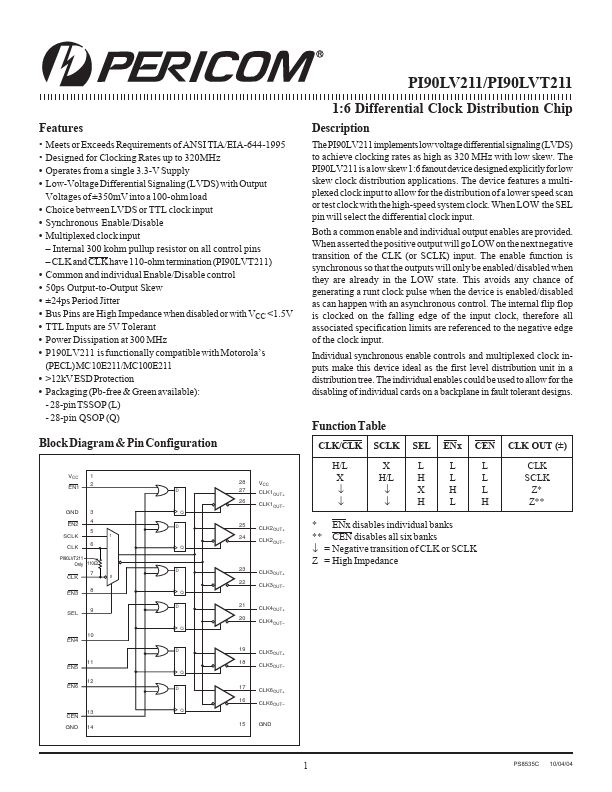
The PI90LV211 implements low voltage differential signaling (LVDS) to achieve clocking rates as high as 320 MHz with low skew. The PI90LV211 is a low skew 1:6 fanout device designed explicitly for low skew clock distribution applications.
- Meets or Exceeds Requirements of ANSI TIA/EIA-644-1995 Designed for Clocking Rates up to 320MHz Operates from a single 3.3-V Supply Low-Voltage Differential Signaling (LVDS) with Output Voltages of ±350mV into a 100-ohm load Choice between LVDS or TTL clock input Synchronous Enable/Disable Multiplexed clock input - Internal 300 kohm pullup resistor on all control pins - CLK and CLK have 110-ohm termination (PI90LVT211) Common and individual Enable/Disable control 50ps Output-to-Output Skew ±24ps Period Jitter Bus Pins are High Impedance when disabled or with VCC <1.5V TTL Inputs are 5V Tolerant Power Dissipation at 300 MHz P190LV211 is functionally compatible with Motorola’s (PECL) MC 10E211/MC100E211 >12kV ESD Protection Packaging (Pb-free & Green available): - 28-pin TSSOP (L) - 28-pin QSOP (Q)