PDM6ET20V08E Overview
Description
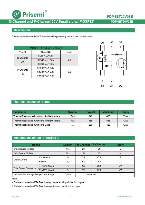
The enhancement mode MOS is extremely high density cell and low on-resistance. MOSFET Product Summary VDS(V) RDS(on)(Ω) N-Channel 20 0.2@ VGS=4.5V 0.25@ VGS=2.5V 0.31@ VGS=1.8V P-Channel -20 0.45@ VGS=-4.5V 0.62@ VGS=-2.5V 0.86@ VGS=-1.8V ID(A) 0.8 -0.8 PDM6ET20V08E PDM6ET20V08E D1 G2 S2 6 5 4 1 2 3 S1 G1 D2 Parameter Symbol RθJA RθJA RθJC Typical 340 465 280 Maximum 430 555 320 Units ℃/W ℃/W ℃/W Absolute maximum rating@25℃ Rating Symbol N-Channel P-Channel Drain-Source Voltage VDS 20 -20 Gate-Source Voltage VGS ±8 ±8 Drain Current Continuous Pulsed ID 0.8 -0.8 ID 3.0 -3.0 TA=25℃,Note:a PD 290 290 Total Power Dissipation TA=25℃,Note:b PD 220 220 Junction and Storage Temperature Range TJ,TSTG -55~+150 Note a:Surface mounted on FR4 Board using 1 square inch pad size,1oz copper b:Surface mounted on FR4 Board using minimum pad size,1oz copper Rev.06.4 1 Units V V A A mW mW ℃ N-Channel and P-Channel,20V,Small signal MOSFET PDM6ET20V08E - N-Channel Parameter Drain-Source Breakdown Voltage Zero Gate Voltage Drain Current Gate-Body Leakage Current Gate Threshold Voltage Symbol BVDSS IDSS IGSS VGS(th) Static Drain-Source On-Resistance RDS(ON) Forward transfer admittance Input Capacitance Output Capacitance Reverse Transfer Capacitance Total Gate Charge Gate-Source Charge Gate-Drain Charge Turn-On Delay Time Turn-Off Delay Time Turn-On Rise Time Turn-On Fall Time Drain-Source Diode Forward Voltage gFS CISS COSS CRSS QG QGS QGD td(on) td(off) tr tf VSD Conditions ID =1mA,VGS=0V VDS =20V,VGS=0V VDS =0V,VGS=±8V VDS = VGS , ID =250μA VGS=4.5V, ID =0.65A VGS=2.5V, ID =0.45A VGS=1.8V, ID =0.25A.