PNM8P30V20 Overview
Description
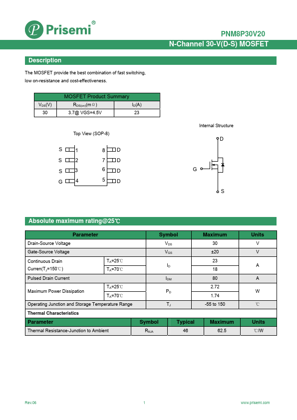
The MOSFET provide the best combination of fast switching, low on-resistance and cost-effectiveness. VDS(V) 30 MOSFET Product Summary RDS(on)(mΩ) ID(A) 3.7@ VGS=4.5V 23 Top View (SOP-8) S1 S2 S3 G4 8D 7D 6D 5D PNM8P30V20 N-Channel 30-V(D-S) MOSFET Internal Structure D G S Absolute maximum rating@25℃ Parameter Drain-Source Voltage Gate-Source Voltage Continuous Drain Curren(TJ=150℃) Pulsed Drain Current TA=25℃ TA=70℃ Maximum Power Dissipation TA=25℃ TA=70℃ Operating Junction and Storage Temperature Range Parameter Symbol VDS VGS ID IDM PD TJ Symbol RθJA Typical 46 Maximum 30 ±20 23 18 80 2.72 1.74 -55 to 150 Maximum 62.5 Units V V A A W ℃ Units ℃/W Rev.06 1 N-Channel 30-V(D-S) MOSFET PNM8P30V20 Parameter Drain-Source Breakdown Voltage Zero Gate Voltage Drain Current Gate-Body Leakage Current Gate Threshold Voltage Static Drain-Source On-Resistance Drain-Source Diode Forward Voltage Total Gate Charge Total Gate Charge Gate-Source Charge Gate-Drain Charge Input Capacitance Output Capacitance Reverse Transfer Capacitance Turn-On Delay Time Turn-Off Delay Time Turn-On Rise Time Turn-On Fall Time Gate-Resistance Symbol BVDSS IDSS IGSS VGS(th) RDS(ON) VSD Qg Qg Qgs Qgd CISS COSS CRSS td(on) td(off) tr tf Rg Conditions ID =250μA,VGS=0V VDS =20V,VGS=0V VDS =0V,VGS=±20V VDS =VGS, ID =250μA VGS=10V, ID =15A VGS=4.5V, ID =10A VGS=0V,IS=15A VGS=4.5V, VDS =15V, ID =10A VGS=10V, VDS =15V, ID =10A VGS=0V, VDS =15V, f=1MHz VDD =15V, VGEN =10V, RG=1Ω,RL=15Ω ID =1A VGS=0V, VDS =0V,f=1MHz Min.