PNMT60V02 Overview
Description
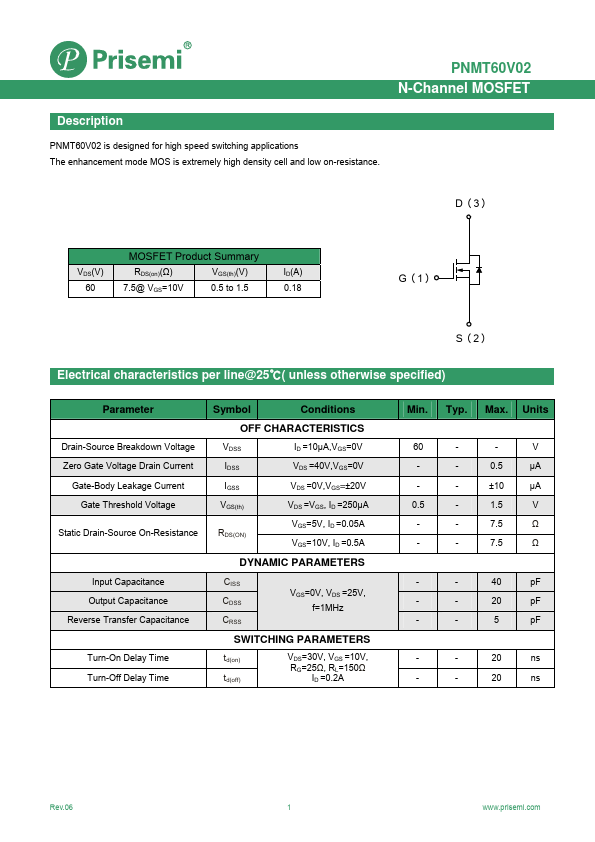
PNMT60V02 is designed for high speed switching applications The enhancement mode MOS is extremely high density cell and low on-resistance. D(3) VDS(V) 60 MOSFET Product Summary RDS(on)(Ω) VGS(th)(V) 7.5@ VGS=10V 0.5 to 1.5 ID(A) 0.18 G(1) S(2) Parameter Drain-Source Breakdown Voltage Zero Gate Voltage Drain Current Gate-Body Leakage Current Gate Threshold Voltage Static Drain-Source On-Resistance Input Capacitance Output Capacitance Reverse Transfer Capacitance Turn-On Delay Time Turn-Off Delay Time Symbol Conditions OFF CHARACTERISTICS VDSS IDSS IGSS VGS(th) RDS(ON) ID =10μA,VGS=0V VDS =40V,VGS=0V VDS =0V,VGS=±20V VDS =VGS, ID =250μA VGS=5V, ID =0.05A VGS=10V, ID =0.5A DYNAMIC PARAMETERS CISS CDSS CRSS VGS=0V, VDS =25V, f=1MHz SWITCHING PARAMETERS td(on) td(off) VDS=30V, VGS =10V, RG=25Ω, RL=150Ω ID =0.2A Min.