V58C2256404SC Overview
Description
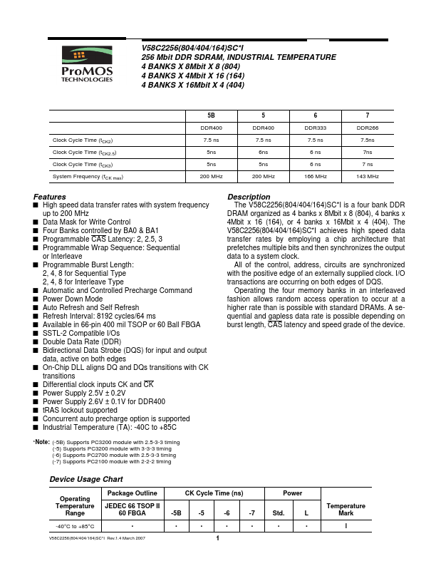
The V58C2256(804/404/164)SC*I is a four bank DDR DRAM organized as 4 banks x 8Mbit x 8 (804), 4 banks x 4Mbit x 16 (164), or 4 banks x 16Mbit x 4 (404). The V58C2256(804/404/164)SC*I achieves high speed data transfer rates by employing a chip architecture that prefetches multiple bits and then synchronizes the output data to a system clock.
Key Features
- High speed data transfer rates with system frequency up to 200 MHz
- Data Mask for Write Control
- Four Banks controlled by BA0 & BA1
- Programmable CAS Latency: 2, 2.5, 3
- Programmable Wrap Sequence: Sequential or Interleave