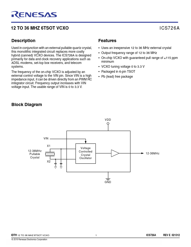
ICS726A
12 TO 36 MHZ 6TSOT VCXO
Pin Assignment
X2 1
GND 2
CLK 3
6 X1
5 VIN
4 VDD
TSOT- 2 3- 6
VCXO
Pin Descriptions
Pin
Number
1
2
3
4
5
6
Pin
Name
X2
GND
CLK
VDD
VIN
XI
Pin
Type
Pin Description
Input Crystal connection. Connect to the external pullable crystal.
Power Connect to ground.
Output VCXO CMOS level clock output at the frequency of the crystal.
Power Connect to +3.3 V (0.01µf decoupling capacitor recommended).
Input Voltage input to VCXO — 0 to 3.3 V analog input which controls the
oscillation frequency of the VCXO.
Input Crystal connection. Connect to the external pullable crystal.
External Component Selection
The ICS726A requires a minimum number of external
components for proper operation.
Decoupling Capacitor
A decoupling capacitor of 0.01µF must be connected
between VDD (pin 4) and GND (pin 2), as close to these
pins as possible. For optimum device performance, the
decoupling capacitor should be mounted on the component
side of the PCB. Avoid the use of vias in the decoupling
circuit.
Series Termination Resistor
When the PCB trace between the clock output (CLK, pin 3)
and the load is over 1 inch, series termination should be
used. To series terminate a 50Ω trace (a commonly used
trace impedance) place a 33Ω resistor in series with the
clock line, as close to the clock output pin as possible. The
nominal impedance of the clock output is 20Ω.
Quartz Crystal
The ICS726A VCXO function consists of the external crystal
and the integrated VCXO oscillator circuit. To assure the
best system performance (frequency pull range) and
reliability, a crystal device with the recommended
parameters (shown below) must be used, and the layout
guidelines discussed in the following section shown must be
followed.
The frequency of oscillation of a quartz crystal is determined
by its “cut” and by the load capacitors connected to it. The
ICS726A incorporates on-chip variable load capacitors that
“pull” (change) the frequency of the crystal. The crystal
specified for use with the ICS726A is designed to have zero
frequency error when the total of on-chip + stray
capacitance is 8.9 pF.
Required Crystal Parameters:
Nominal Frequency
as required MHz
Initial Accuracy at 25° C
-20 min/+20 max ppm
Temperature Stability
-30 min/+30 max ppm
Aging, 1st year
-5 min/+5 max ppm
Aging, 10 years
-20 min/+20 max ppm
Operating Temp. Range, °C 0 min/+25 typ/+70 max
or
Operating Temp. Range, °C -40 min/+25 typ/+85 max
Load Capacitance
8.6 pf
Shunt Capacitance, C0
7 pF Max
C0/C1 Ratio
270 Max
Equivalent Series Resistance
35 Ω Max
IDT® 12 TO 36 MHZ 6TSOT VCXO
2
ICS726A
REV E 021312