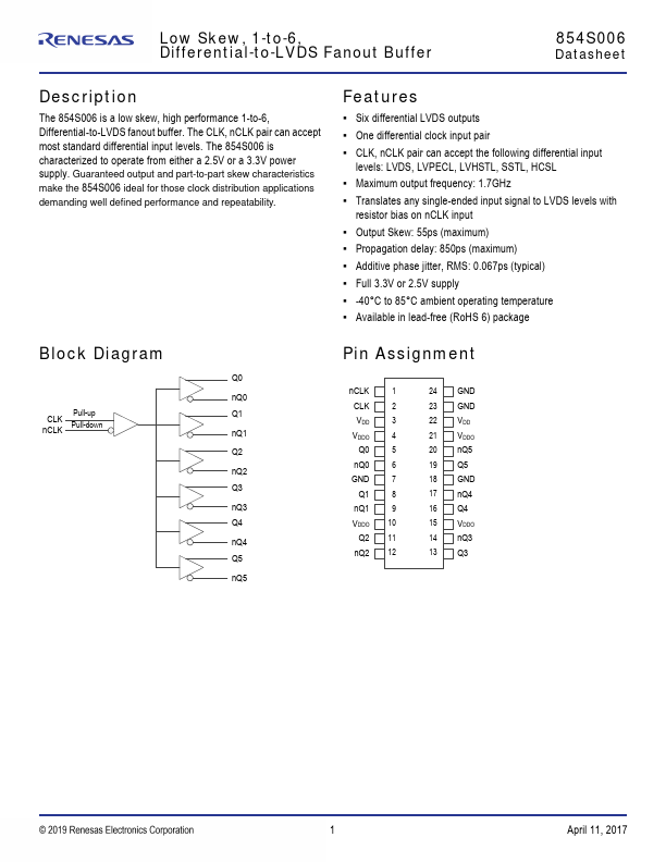
Datasheet4U Logo Datasheet4U.com

854S006 - Differential-to-LVDS Fanout Buffer

General Description

The 854S006 is a low skew, high performance 1-to-6, Differential-to-LVDS fanout buffer.

The CLK, nCLK pair can accept most standard differential input levels.

The 854S006 is characterized to operate from either a 2.5V or a 3.3V power supply.

Key Features

  • Six differential LVDS outputs.
  • One differential clock input pair.
  • CLK, nCLK pair can accept the following differential input levels: LVDS, LVPECL, LVHSTL, SSTL, HCSL.
  • Maximum output frequency: 1.7GHz.
  • Translates any single-ended input signal to LVDS levels with resistor bias on nCLK input.
  • Output Skew: 55ps (maximum).
  • Propagation delay: 850ps (maximum).
  • Additive phase jitter, RMS: 0.067ps (typical).
  • Full 3.3V or 2.5V supply.
  • -40°C to 85°C ambien.

📥 Download Datasheet

Datasheet Details

Part number 854S006
Manufacturer Renesas
File Size 1.04 MB
Description Differential-to-LVDS Fanout Buffer
Datasheet download datasheet 854S006 Datasheet

Full PDF Text Transcription (Reference)

The following content is an automatically extracted verbatim text from the original manufacturer datasheet and is provided for reference purposes only.

View original datasheet text
Low Skew, 1-to-6, Differential-to-LVDS Fanout Buffer 854S006 Datasheet Description The 854S006 is a low skew, high performance 1-to-6, Differential-to-LVDS fanout buffer. The CLK, nCLK pair can accept most standard differential input levels. The 854S006 is characterized to operate from either a 2.5V or a 3.3V power supply. Guaranteed output and part-to-part skew characteristics make the 854S006 ideal for those clock distribution applications demanding well defined performance and repeatability. Features ▪ Six differential LVDS outputs ▪ One differential clock input pair ▪ CLK, nCLK pair can accept the following differential input levels: LVDS, LVPECL, LVHSTL, SSTL, HCSL ▪ Maximum output frequency: 1.