9DMV0131B
9DMV0131B is 2:1 1.8V PCIe Gen1-5 Clock Mux manufactured by Renesas.
Description
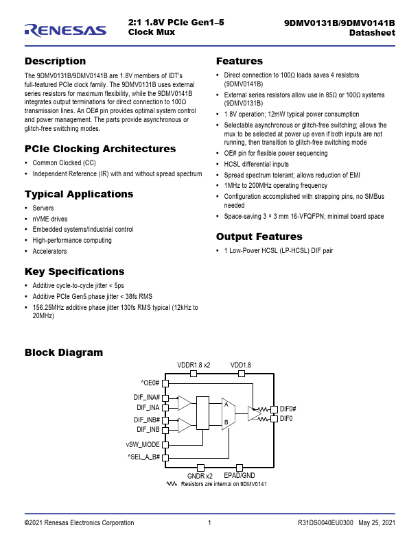
The 9DMV0131B/9DMV0141B are 1.8V members of IDT’s full-featured PCIe clock family. The 9DMV0131B uses external series resistors for maximum flexibility, while the 9DMV0141B integrates output terminations for direct connection to 100Ω transmission lines. An OE# pin provides optimal system control and power management. The parts provide asynchronous or glitch-free switching modes.
PCIe Clocking Architectures
- mon Clocked (CC)
- Independent Reference (IR) with and without spread spectrum
Typical Applications
- Servers
- n VME drives
- Embedded systems/Industrial control
- High-performance puting
- Accelerators
Features
- Direct connection to 100Ω loads saves 4 resistors (9DMV0141B)
- External series resistors allow use in 85Ω or 100Ω systems (9DMV0131B)
- 1.8V operation; 12m W typical power consumption
- Selectable asynchronous or glitch-free switching; allows the mux to be selected at power up even if both inputs are not running, then transition to glitch-free switching mode
- OE# pin for flexible power sequencing
- HCSL differential inputs
- Spread spectrum tolerant; allows reduction of EMI
- 1MHz to 200MHz operating frequency
- Configuration acplished with strapping pins, no SMBus needed
- Space-saving 3 × 3 mm 16-VFQFPN; minimal board space
Output Features
- 1 Low-Power HCSL (LP-HCSL) DIF pair
Key Specifications
- Additive cycle-to-cycle jitter < 5ps
- Additive PCIe Gen5 phase jitter < 38fs RMS
- 156.25MHz additive phase jitter 130fs RMS typical (12k Hz to
20MHz)
Block Diagram
^OE0#
DIF_INA# DIF_INA DIF_INB# DIF_INB v SW_MODE ^SEL_A_B#
VDDR1.8 x2
VDD1.8
DIF0#
DIF0
GNDR x2 EPAD/GND
Resistors are internal on...