9FGL0251 Overview
Description
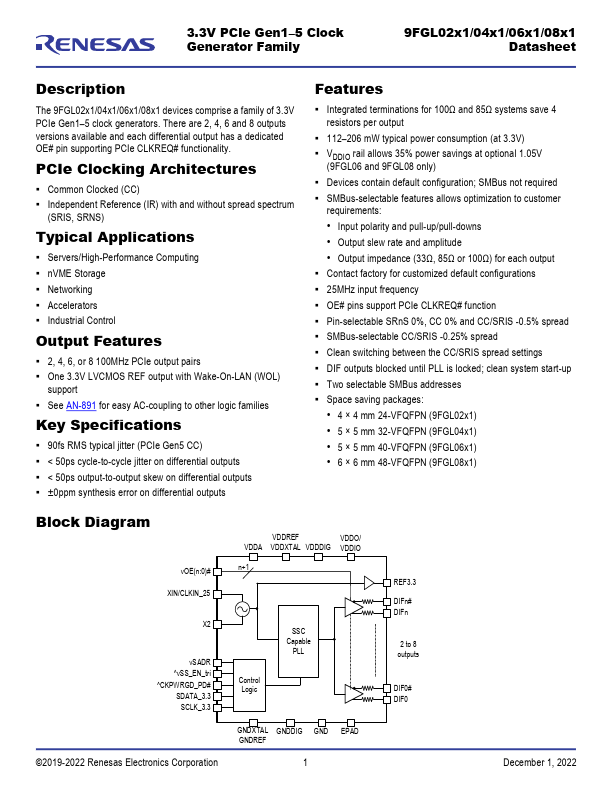
The 9FGL02x1/04x1/06x1/08x1 devices comprise a family of 3.3V PCIe Gen1–5 clock generators. There are 2, 4, 6 and 8 outputs versions available and each differential output has a dedicated OE# pin supporting PCIe CLKREQ# functionality.
Key Features
- Input polarity and pull-up/pull-downs
- Output slew rate and amplitude