9FGV0841 Overview
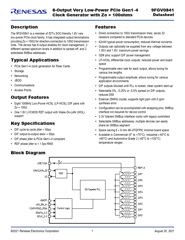
The 9FGV0841 is a member of IDT's SOC-friendly 1.8V very low-power PCIe clock family. It has integrated output terminations providing Zo = 100Ω for direction connection to 100Ω transmission lines. The device has 8 output enables for clock management, 2 different spread spectrum levels in addition to spread off, and 2 selectable SMBus addresses.
9FGV0841 Key Features
- Eight 100MHz Low-Power HCSL (LP-HCSL) DIF pairs with Zo = 100Ω
- One 1.8V LVCMOS REF output with Wake-On-LAN (WOL) support
- DIF cycle-to-cycle jitter < 50ps
- DIF output-to-output skew < 50ps
- DIF phase jitter is PCIe Gen1-4 pliant
- REF phase jitter is < 1.5ps RMS
- Direct connection to 100Ω transmission lines; saves 32 resistors pared to standard PCIe devices
- 62mW typical power consumption; reduced thermal concerns
- Outputs can optionally be supplied from any voltage between
- OE# pins; support DIF power management
9FGV0841 Applications
- PCIe Gen1-4 clock generation for Riser Cards