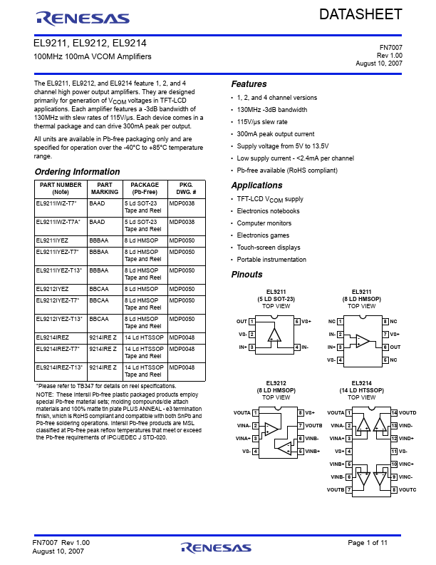
EL9211, EL9212, EL9214
Absolute Maximum Ratings (TA = +25°C)
Supply Voltage between VS+ and VS- . . . . . . . . . . . . . . . . . . . .+15V
Input Voltage . . . . . . . . . . . . . . . . . . . . . . . . . . VS- - 0.5V, VS +0.5V
Maximum Continuous Output Current . . . . . . . . . . . . . . . . . . 100mA
Ambient Operating Temperature . . . . . . . . . . . . . . . .-40°C to +85°C
Thermal Information
Power Dissipation . . . . . . . . . . . . . . . . . . . . . . . . . . . . . See Curves
Maximum Die Temperature . . . . . . . . . . . . . . . . . . . . . . . . . . +125°C
Storage Temperature . . . . . . . . . . . . . . . . . . . . . . . .-65°C to +150°C
Pb-free reflow profile . . . . . . . . . . . . . . . . . . . . . . . . . .see link below
http://www.intersil.com/pbfree/Pb-FreeReflow.asp
CAUTION: Do not operate at or near the maximum ratings listed for extended periods of time. Exposure to such conditions may adversely impact product reliability and
result in failures not covered by warranty.
IMPORTANT NOTE: All parameters having Min/Max specifications are guaranteed. Typ values are for information purposes only. Unless otherwise noted, all tests are
at the specified temperature and are pulsed tests, therefore: TJ = TC = TA
Electrical Specifications VS+ = +6V, VS- = -6V, RL = 10k, RF = 0, CL = 10pF to 0V, Gain = -1, TA = +25°C, unless otherwise
specified.
PARAMETER
DESCRIPTION
CONDITIONS
MIN MAX
(Note 2) TYP (Note 2) UNIT
INPUT CHARACTERISTICS
VOS
TCVOS
IB
RIN
CIN
VREG
CMIR
Input Offset Voltage
Average Offset Voltage Drift
Input Bias Current
Input Impedance
Input Capacitance
Load Regulation
Common Mode Input Range
VCM = 6V
(Note 1)
VCM = 6V
VCOM = 6V, -100mA < IL < 100mA
-6 -1 +2 mV
10 µV/C
-1.4 -0.4 µA
1 G
1.35 pF
-20 +20 mV
-0.5
+12.5
V
CMRR
Common Mode Rejection Ratio
AVOL
Open Loop Gain
OUTPUT CHARACTERISTICS
For VIN from -0.5 to +12.5V
75 100
55 70
dB
dB
VOL Output Swing Low
VOH
Output Swing High
ISC Short Circuit Current
POWER SUPPLY PERFORMANCE
IL = -5mA
IL = +5mA
0.9
10.7 10.94
300
1.1
V
V
mA
PSRR
IS
Power Supply Rejection Ratio
Total Supply Current
VS from 4.5V to 10.5V
EL9211 (no load)
EL9212 (no load)
50 75
dB
2.3 2.9 mA
4.5 5 mA
EL9214 (no load)
8.8 9.6 mA
DYNAMIC PERFORMANCE
SR Slew Rate (Note)
2V step, 20% to 80%
90 115
V/µs
tS Settling to +0.1% (AV = -1) (AV = -1), VO = 2V step
30
BW -3dB Bandwidth
RL = 10k, CL = 10pF, AV = +1
130
RL = 10k, CL = 10pF, AV = -1
52
GBWP
Gain-Bandwidth Product
RL = 10k, CL = 10pF
63
PM Phase Margin
RL = 10k, CL = 10pF
43
NOTE:
1. Slew rate is measured on rising and falling edges.
2. Parts are 100% tested at +25°C. Over-temperature limits established by characterization and are not production tested.
ns
MHz
MHz
MHz
°
FN7007 Rev 1.00
August 10, 2007
Page 2 of 11