HIP2123 Overview
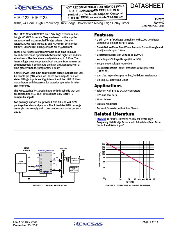
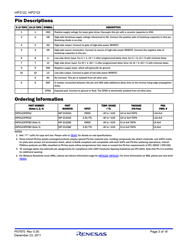
They are based on the popular ISL2100A and ISL2101A half-bridge drivers. Like the ISL2100A, two logic inputs, LI and HI, control both bridge outputs, LO and HO. All logic inputs are VDD tolerant.
HIP2123 Key Features
- 9 Ld TDFN “B” Package pliant with 100V Conductor Spacing Guidelines per IPC-2221
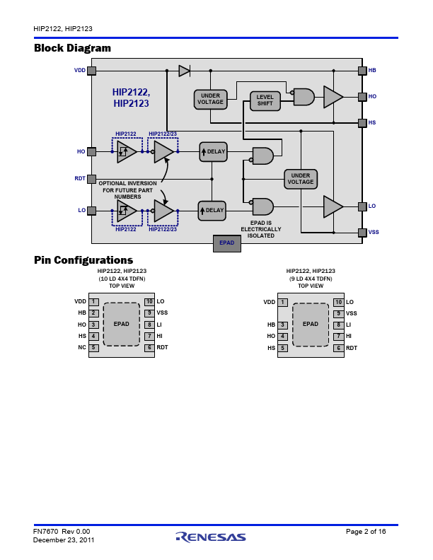
- Break-Before-Make Dead-Time Prevents Shoot-through and is adjustable up to 220ns
- Bootstrap Supply Max Voltage to 114VDC
- Wide Supply Voltage Range (8V to 14V)
- Supply Undervoltage Protection
- CMOS patible Input Thresholds with Hysteresis (HIP2122)
- 1.6/1 Typical Output Pull-up/Pull-down Resistance
- On-Chip 1Ω Bootstrap Diode