ICS252BI09L Description
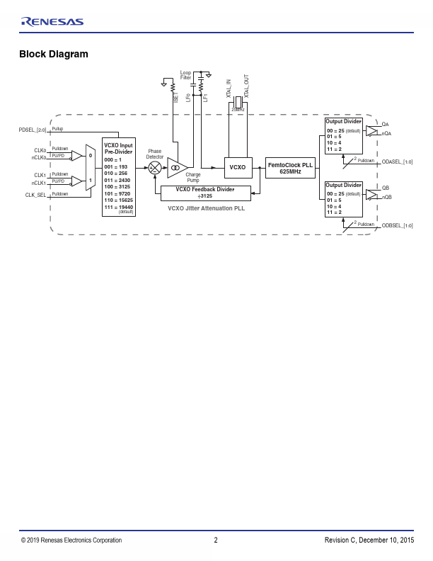
The 813N252I-09 is a PLL based synchronous multiplier that is optimized for PDH or SONET to Ethernet clock jitter attenuation and frequency translation. The device contains two internal frequency multiplication stages that are cascaded in series. The first stage is a VCXO PLL that is optimized to provide reference clock jitter attenuation.
ICS252BI09L Key Features
- Two LVPECL output pairs
- Two differential inputs support the following input types: LVPECL
- Accepts input frequencies from 8kHz to 155.52MHz including
- Attenuates the phase jitter of the input clock by using a low-cost
- VCXO PLL bandwidth can be optimized for jitter attenuation and
- FemtoClock frequency multiplier provides low jitter, high frequency
- Absolute pull range: 50ppm
- FemtoClock VCO frequency: 625MHz
- RMS phase jitter @ 125MHz, using a 25MHz crystal
- 20MHz): 0.25ps (typical) and 0.35ps (maximum)