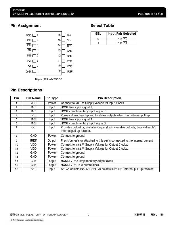
Datasheet4U Logo Datasheet4U.com

ICS557-08 Datasheet - Renesas

2:1 MULTIPLEXER

ICS557-08 Features

* Packaged in 16-pin TSSOP

* Pb (lead) free package

* Operating voltage of 3.3 V

* Low power consumption

* Input clock frequency of up to 200 MHz

* For PCIe Gen2/3 applications, see the 5V41068A Block Diagram VDD OE 3 IN1 IN1 CLK MUX IN2 2 to

ICS557-08 General Description

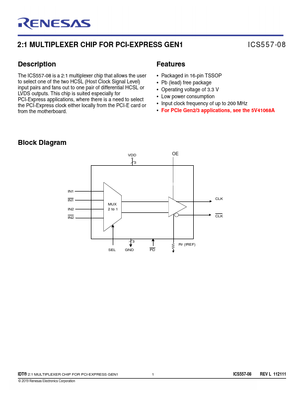
The ICS557-08 is a 2:1 multiplexer chip that allows the user to select one of the two HCSL (Host Clock Signal Level) input pairs and fans out to one pair of differential HCSL or LVDS outputs. This chip is suited especially for PCI-Express applications, where there is a need to select the PCI-Express.

ICS557-08 Datasheet (287.33 KB)

Preview of ICS557-08 PDF

Datasheet Details

Part number:

ICS557-08

Manufacturer:

Renesas ↗

File Size:

287.33 KB

Description:

2:1 multiplexer.

📁 Related Datasheet

ICS557-01 PCI-EXPRESS GEN1 CLOCK SOURCE (Renesas)

ICS557-01 PCI-EXPRESS CLOCK SOURCE (ICST)

ICS557-03 spread spectrum clock generator (Renesas)

ICS557-03 2 OUTPUT PCI-EXPRESS GEN1 CLOCK SOURCE (Renesas)

ICS557-03 spread spectrum clock generator (IDT)

ICS557-05A spread-spectrum clock generator (Renesas)

ICS557-05A Quad Differential PCI-Express Clock Source (ICST)

ICS557-06 2 TO 4 DIFFERENTIAL PCIE GEN1 CLOCK MUX (Renesas)

ICS557-06 ONE TO FOUR HCSL CLOCK BUFFER (ICST)

ICS557-08 2:1 MULTIPLEXER CHIP (ICST)

TAGS

ICS557-08 MULTIPLEXER Renesas

Image Gallery

ICS557-08 Datasheet Preview Page 2 ICS557-08 Datasheet Preview Page 3

ICS557-08 Distributor