ICS726A Description
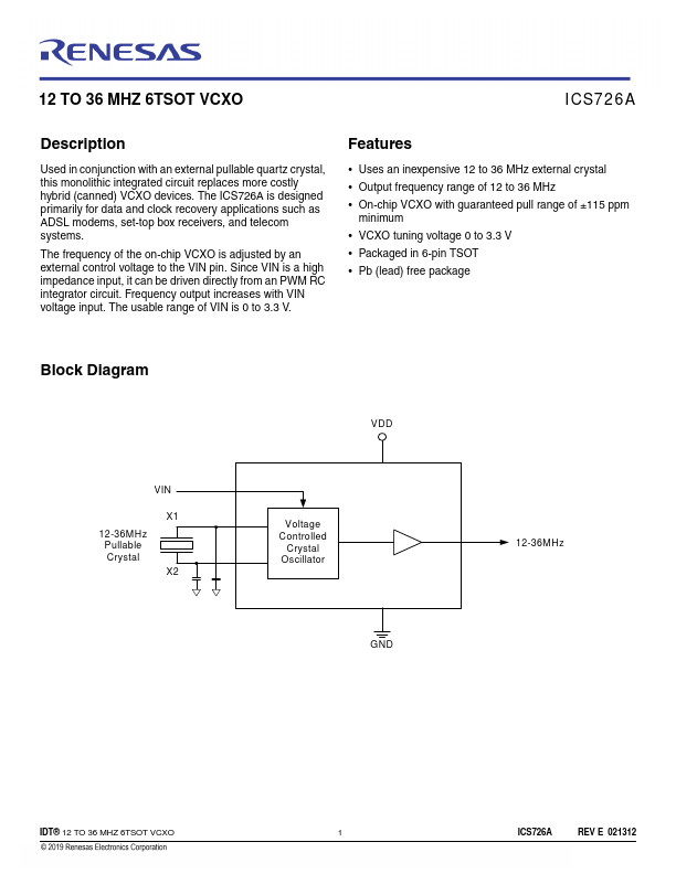
Used in conjunction with an external pullable quartz crystal, this monolithic integrated circuit replaces more costly hybrid (canned) VCXO devices. The ICS726A is designed primarily for data and clock recovery applications such as ADSL modems, set-top box receivers, and tele systems. The frequency of the on-chip VCXO is adjusted by an external control voltage to the VIN pin.
ICS726A Key Features
- Uses an inexpensive 12 to 36 MHz external crystal
- Output frequency range of 12 to 36 MHz
- On-chip VCXO with guaranteed pull range of ±115 ppm
- VCXO tuning voltage 0 to 3.3 V
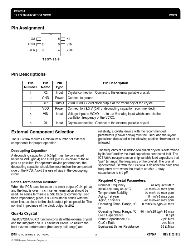
- Packaged in 6-pin TSOT
- Pb (lead) free package
- 0 to 3.3 V analog input which controls the oscillation frequency of the VCXO
ICS726A Applications
- Uses an inexpensive 12 to 36 MHz external crystal
- Output frequency range of 12 to 36 MHz
- On-chip VCXO with guaranteed pull range of ±115 ppm
- VCXO tuning voltage 0 to 3.3 V
- Packaged in 6-pin TSOT


